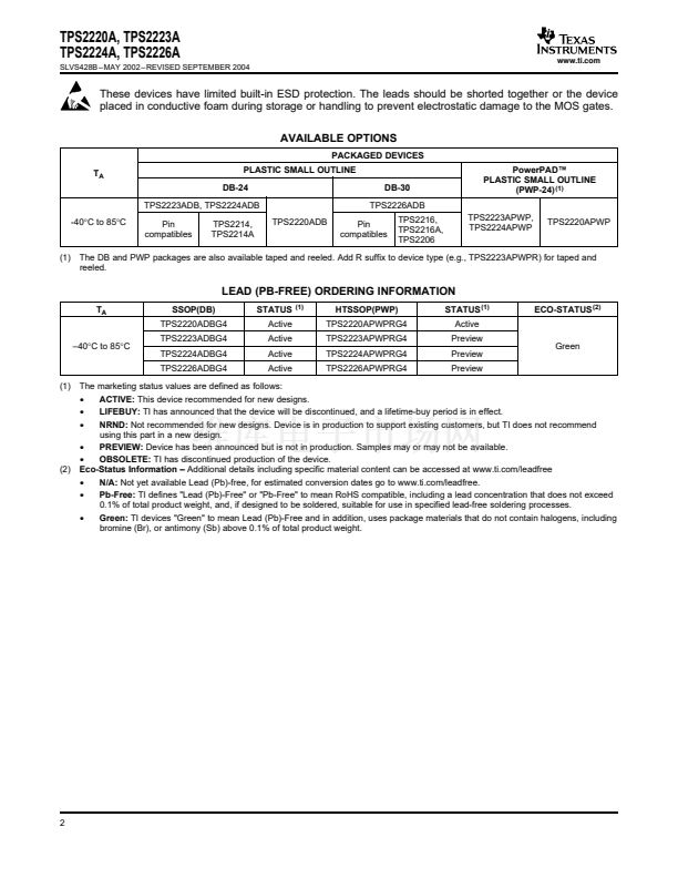
www.ti.com
TPS2220A, TPS2223A
TPS2224A, TPS2226A
SLVS428B 鈥?MAY 2002 鈥?REVISED SEPTEMBER 2004
APPLICATION INFORMATION (continued)
0.1-碌F ceramic capacitor. It is strongly recommended that the switched outputs be bypassed with a 0.1-碌F (or
larger) ceramic capacitor; doing so improves the immunity of the IC to electrostatic discharge (ESD). Care should
be taken to minimize the inductance of PCB traces between the devices and the load. High switching currents
can produce large negative voltage transients, which forward biases substrate diodes, resulting in unpredictable
performance. Similarly, no pin should be taken below -0.3 V.
RESET INPUT
To ensure that cards are in a known state after power brownouts or system initialization, the PC Cards should be
reset at the same time as the host by applying low-impedance paths from xVCC and xVPP terminals to ground.
A low-impedance output state allows discharging of residual voltage remaining on PC Card filter capacitance,
permitting the system (host and PC Cards) to be powered up concurrently. The active low RESET input closes
internal ground switches S1, S4, S7, and S11 with all other switches left open. The TPS2220A, TPS2223A,
TPS2224A, and TPS2226A remain in the low-impedance output state until the signal is deasserted and further
data is clocked in and latched. The input serial data cannot be latched during reset mode. RESET is provided for
direct compatibility with systems that use an active-low reset voltage supervisor. The RESET pin has an internal
150-k鈩?pullup resistor.
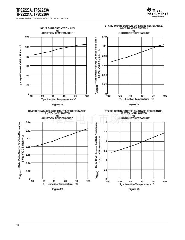
CALCULATING JUNCTION TEMPERATURE
The switch resistance, r
DS(on)
, is dependent on the junction temperature, T
J
, of the die. The junction temperature
is dependent on both r
DS(on)
and the current through the switch. To calculate T
J
, first find r
DS(on)
from Figure 26
through Figure 28, using an initial temperature estimate about 30掳C above ambient. Then, calculate the power
dissipation for each switch, using the formula:
P
+
r
I2
D
DS(on)
Next, sum the power dissipation of all switches and calculate the junction temperature:
T +
P
R
)T
J
D
qJA
A
where:
R
胃JA
is the inverse of the derating factor given in the dissipation rating table.
Compare the calculated junction temperature with the initial temperature estimate. If the temperatures are not
within a few degrees of each other, recalculate using the calculated temperature as the initial estimate.
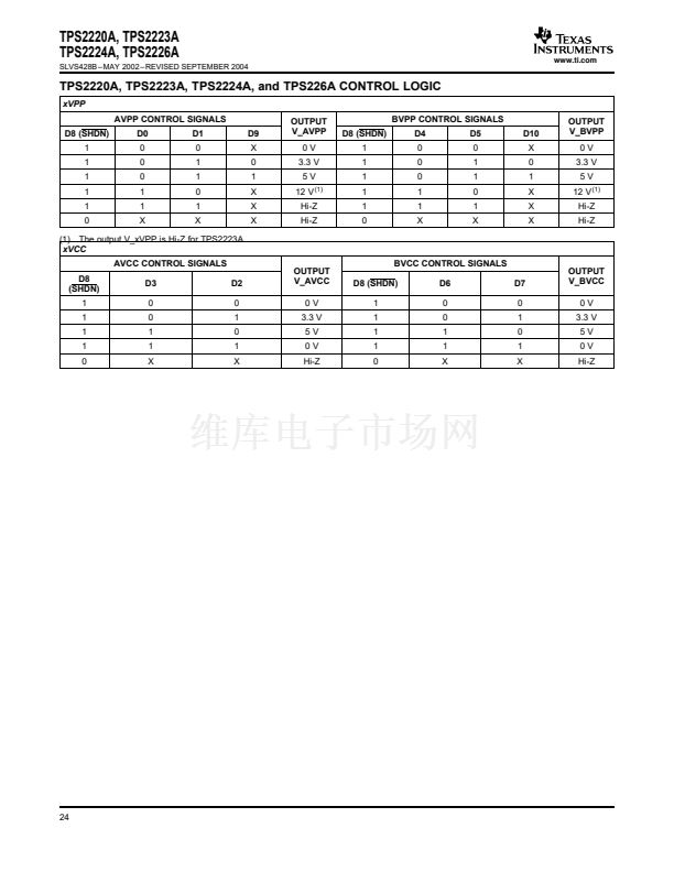
LOGIC INPUTS AND OUTPUTS
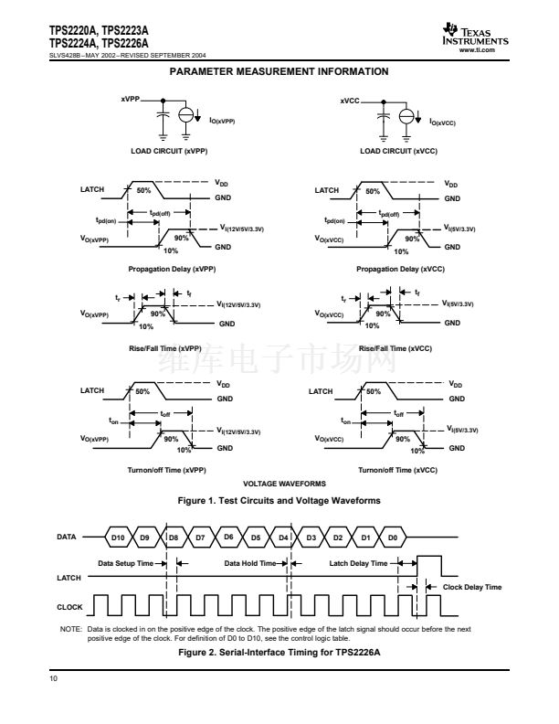
The serial interface consists of the DATA, CLOCK, and LATCH leads. The data is clocked in on the positive
edge of the clock (see Figure 2). The 11-bit (D0-D10) serial data word is loaded during the positive edge of the
latch signal. The positive edge of the latch signal should occur before the next positive edge of the clock occurs.
The serial interface of the device is compatible with serial-interface PCMCIA controllers.
An overcurrent output (OC) is provided to indicate an overcurrent or overtemperature condition in any of the
xVCC and xVPP outputs as previously discussed.
23


 1
1
 2
2
 3
3
 4
4
 5
5
 6
6
 7
7
 8
8
 9
9
 10
10
 11
11
 12
12
 13
13
 14
14
 15
15
 16
16
 17
17
 18
18
 19
19
 20
20
 21
21
 22
22
 23
23
 24
24
 25
25
 26
26
 27
27
 28
28
 29
29
