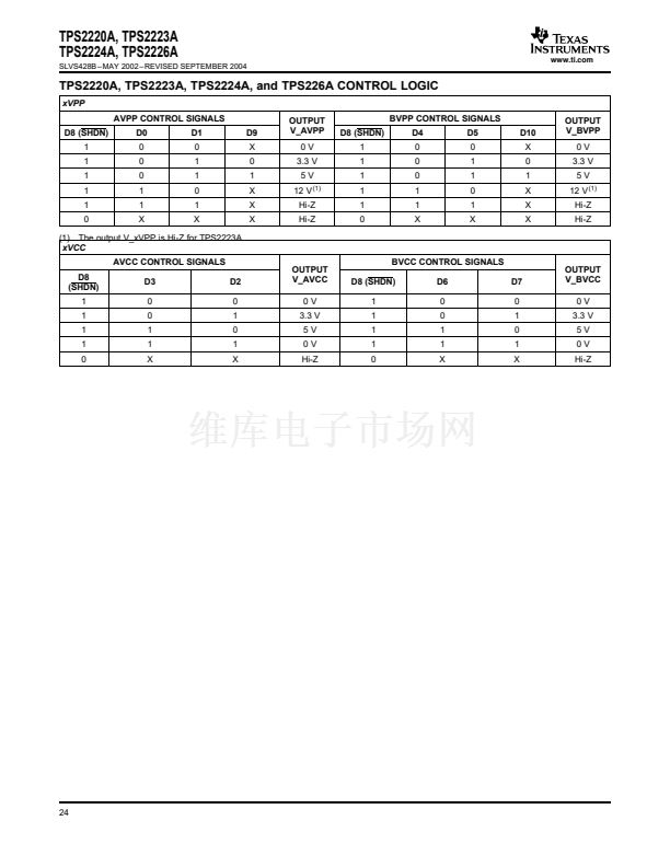
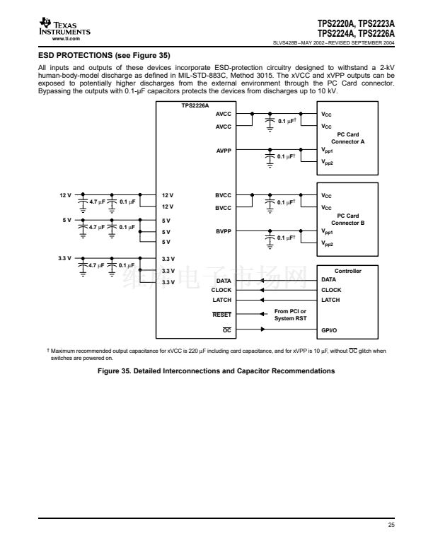
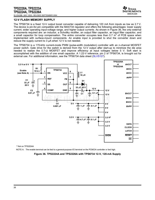
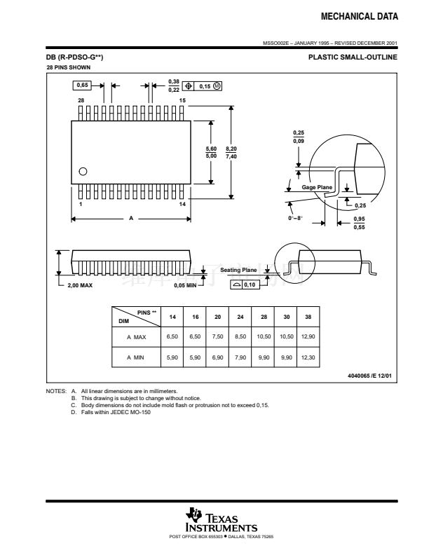
www.ti.com
TPS2220A, TPS2223A
TPS2224A, TPS2226A
SLVS428B 鈥?MAY 2002 鈥?REVISED SEPTEMBER 2004
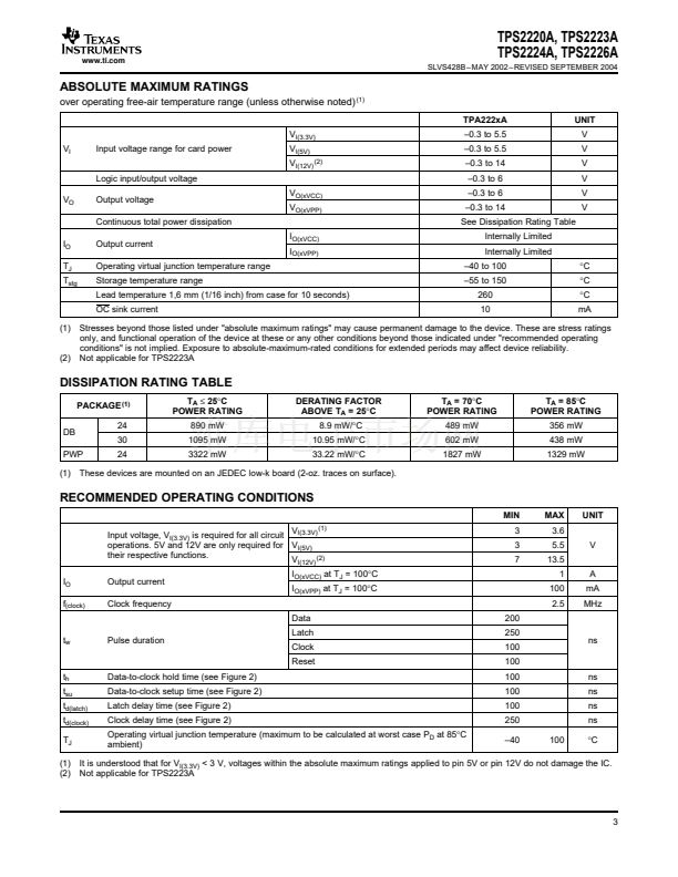
ABSOLUTE MAXIMUM RATINGS
over operating free-air temperature range (unless otherwise noted)
(1)
TPA222xA
V
I(3.3V)
V
I
Input voltage range for card power
Logic input/output voltage
V
O
Output voltage
Continuous total power dissipation
I
O
T
J
T
stg
Output current
Operating virtual junction temperature range
Storage temperature range
Lead temperature 1,6 mm (1/16 inch) from case for 10 seconds)
OC sink current
(1)
(2)
I
O(xVCC)
I
O(xVPP)
V
O(xVCC)
V
O(xVPP)
V
I(5V)
V
I(12V) (2)
鈥?.3 to 5.5
鈥?.3 to 5.5
鈥?.3 to 14
鈥?.3 to 6
鈥?.3 to 6
鈥?.3 to 14
See Dissipation Rating Table
Internally Limited
Internally Limited
鈥?0 to 100
鈥?5 to 150
260
10
掳C
掳C
掳C
mA
UNIT
V
V
V
V
V
V
Stresses beyond those listed under "absolute maximum ratings" may cause permanent damage to the device. These are stress ratings
only, and functional operation of the device at these or any other conditions beyond those indicated under "recommended operating
conditions" is not implied. Exposure to absolute-maximum-rated conditions for extended periods may affect device reliability.
Not applicable for TPS2223A
DISSIPATION RATING TABLE
PACKAGE
(1)
DB
PWP
(1)
24
30
24
T
A
鈮?/div>
25掳C
POWER RATING
890 mW
1095 mW
3322 mW
DERATING FACTOR
ABOVE T
A
= 25掳C
8.9 mW/掳C
10.95 mW/掳C
33.22 mW/掳C
T
A
= 70掳C
POWER RATING
489 mW
602 mW
1827 mW
T
A
= 85掳C
POWER RATING
356 mW
438 mW
1329 mW
These devices are mounted on an JEDEC low-k board (2-oz. traces on surface).
RECOMMENDED OPERATING CONDITIONS
MIN
V
I(3.3V) (1)
Input voltage, V
I(3.3V)
is required for all circuit
operations. 5V and 12V are only required for V
I(5V)
their respective functions.
V
I(12V) (2)
I
O
f
(clock)
Output current
Clock frequency
Data
t
w
Pulse duration
Latch
Clock
Reset
t
h
t
su
t
d(latch)
t
d(clock)
T
J
(1)
(2)
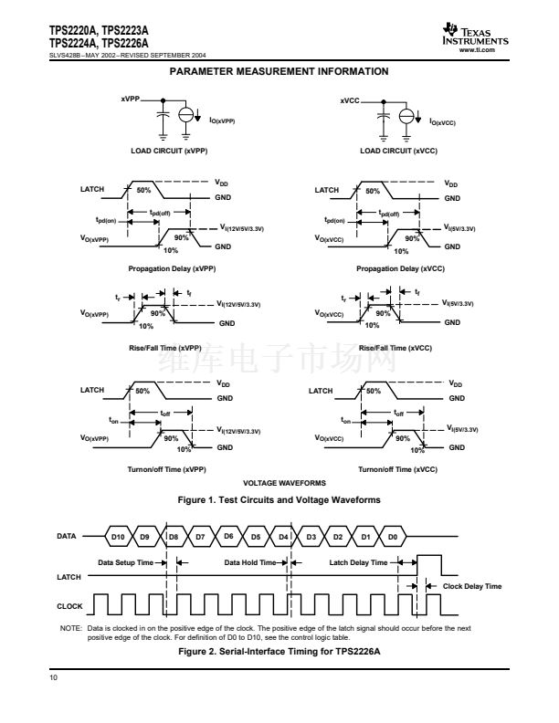
Data-to-clock hold time (see Figure 2)
Data-to-clock setup time (see Figure 2)
Latch delay time (see Figure 2)
Clock delay time (see Figure 2)
Operating virtual junction temperature (maximum to be calculated at worst case P
D
at 85掳C
ambient)
200
250
100
100
100
100
100
250
鈥?0
100
ns
ns
ns
ns
掳C
ns
I
O(xVCC)
at T
J
= 100掳C
I
O(xVPP)
at T
J
= 100掳C
3
3
7
MAX
3.6
5.5
13.5
1
100
2.5
A
mA
MHz
V
UNIT
It is understood that for V
I(3.3V)
< 3 V, voltages within the absolute maximum ratings applied to pin 5V or pin 12V do not damage the IC.
Not applicable for TPS2223A
3


 1
1
 2
2
 3
3
 4
4
 5
5
 6
6
 7
7
 8
8
 9
9
 10
10
 11
11
 12
12
 13
13
 14
14
 15
15
 16
16
 17
17
 18
18
 19
19
 20
20
 21
21
 22
22
 23
23
 24
24
 25
25
 26
26
 27
27
 28
28
 29
29
