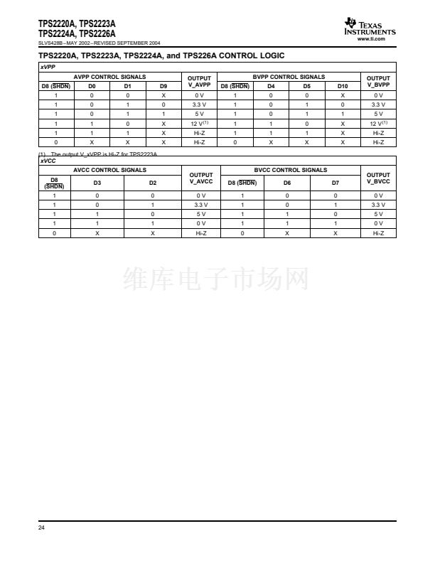
www.ti.com
TPS2220A, TPS2223A
TPS2224A, TPS2226A
SLVS428B 鈥?MAY 2002 鈥?REVISED SEPTEMBER 2004
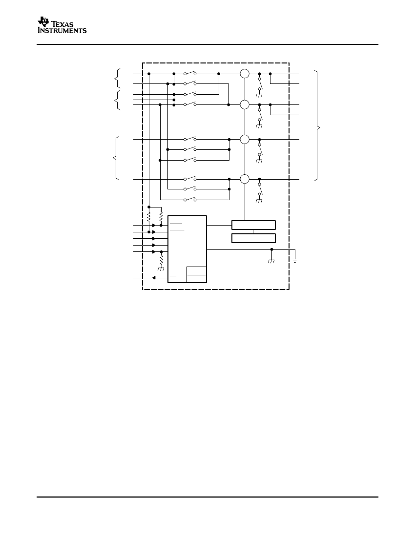
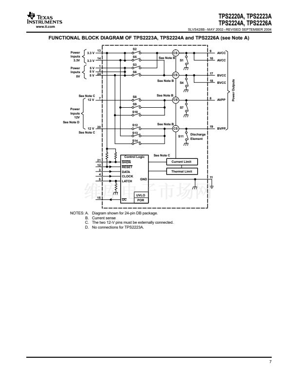
FUNCTIONAL BLOCK DIAGRAM OF TPS2223A, TPS2224A and TPS2226A (see Note A)
Power
Inputs
3.3V
Power
Inputs
5V
3.3 V
3.3 V
13
14
S2
CS
S5
S3
S6
CS
See Note B
S4
17
18
See Note B
S1
9
10
AVCC
AVCC
1
5V
2
5V
24
5V
BVCC
BVCC
Power Outputs
See Note C
12 V
Power
Inputs
12V
See Note D
7
S8
S9
See Note B
CS
S7
8
AVPP
S10
12 V 20
See Note C
S12
S13
See Note B
CS
S11
Discharge
Element
19
BVPP
S14
Control Logic
21
12
3
4
5
SHDN
RESET
DATA
CLOCK
LATCH
GND
See Note C
Current Limit
Thermal Limit
11
15
UVLO
OC
POR
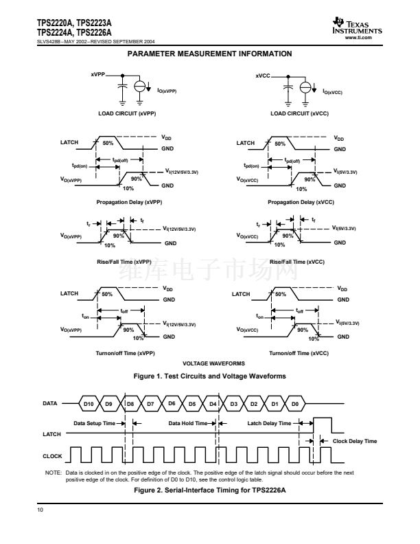
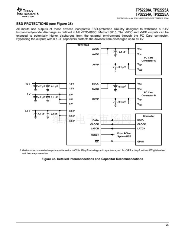
NOTES: A.
B.
C.
D.
Diagram shown for 24-pin DB package.
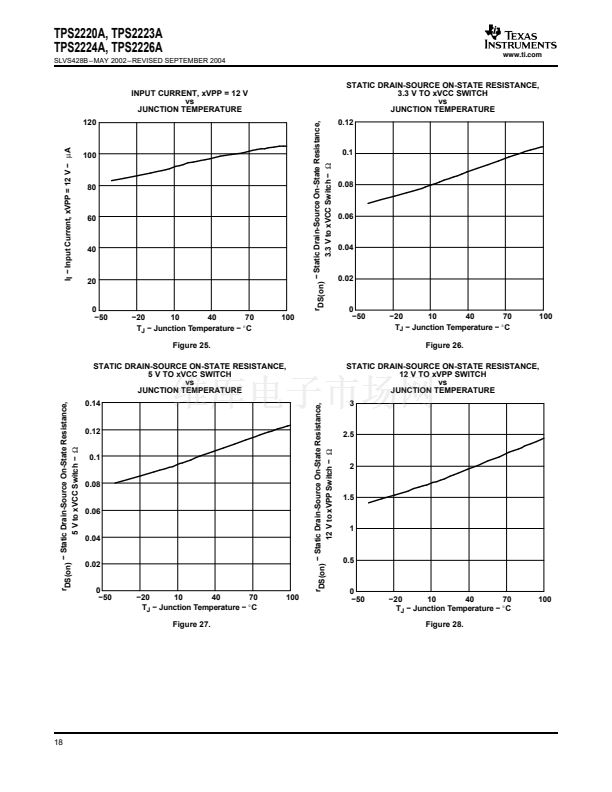
Current sense
The two 12-V pins must be externally connected.
No connections for TPS2223A.
7


 1
1
 2
2
 3
3
 4
4
 5
5
 6
6
 7
7
 8
8
 9
9
 10
10
 11
11
 12
12
 13
13
 14
14
 15
15
 16
16
 17
17
 18
18
 19
19
 20
20
 21
21
 22
22
 23
23
 24
24
 25
25
 26
26
 27
27
 28
28
 29
29
