www.ti.com
TPS61070
TPS61071
SLVS510 鈥?JUNE 2004
APPLICATION INFORMATION
DESIGN PROCEDURE
The TPS6107x dc/dc converters are intended for systems powered by a single-cell, up to triple-cell alkaline,
NiCd, NiMH battery with a typical terminal voltage between 0.9 V and 5.5 V. They can also be used in systems
powered by one-cell Li-ion or Li-polymer with a typical voltage between 2.5 V and 4.2 V. Additionally, any other
voltage source with a typical output voltage between 0.9 V and 5.5 V can power systems where the TPS6107x is
used. Due to the nature of boost converters, only the output voltage regulation is maintained when the input
voltage applied is lower than the programmed output voltage.
Programming the Output Voltage
The output voltage of the TPS61070 dc/dc converter can be adjusted with an external resistor divider. The typical
value of the voltage at the FB pin is 500 mV. The maximum recommended value for the output voltage is 5.5 V.
The current through the resistive divider should be about 100 times greater than the current into the FB pin. The
typical current into the FB pin is 0.01 碌A, and the voltage across R2 is typically 500 mV. Based on those two
values, the recommended value for R2 should be lower than 500 k鈩? in order to set the divider current at 1 碌A or
higher. Because of internal compensation circuitry, the value for this resistor should be in the range of 200 k鈩?
From that, the value of resistor R1, depending on the needed output voltage (V
O
), can be calculated using
Equation 1:
R1
+
R2
O
*
1
V
FB
V
+
180 kW
O
*
1
500 mV
V
(1)
For example, if an output voltage of 3.3 V is needed, a 1-M鈩?resistor should be chosen for R1. If for any reason
the value chosen for R2 is significantly lower than 200 k鈩? additional capacitance in parallel to R1 is
recommended, because the device can show unstable regulation of the output voltage. The required capacitance
value can be calculated using Equation 2:
200 kW
*
1
C
+
3 pF
parR1
R2
(2)
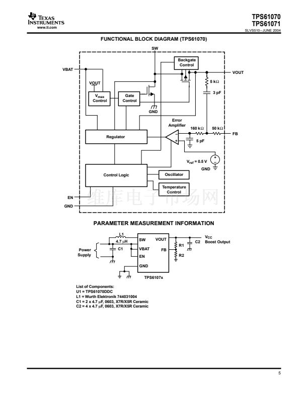
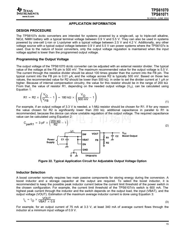
L1
SW
Power
Supply
C1
VBAT
EN
GND
TPS61070
VOUT
R1
FB
R2
C2
V
CC
Boost Output
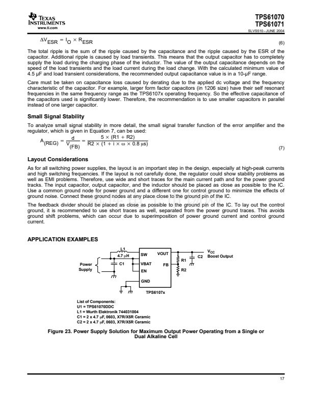
Figure 22. Typical Application Circuit for Adjustable Output Voltage Option
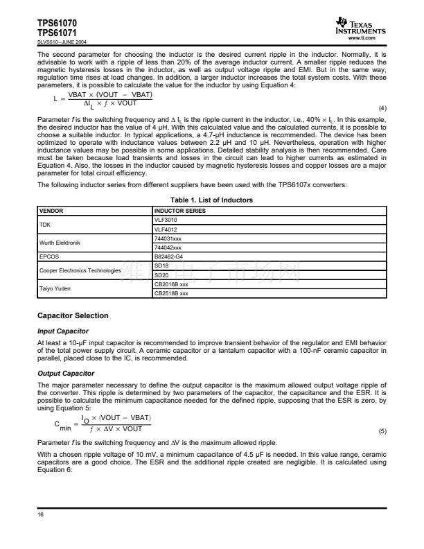
Inductor Selection
A boost converter normally requires two main passive components for storing energy during the conversion. A
boost inductor and a storage capacitor at the output are required. To select the boost inductor, it is
recommended to keep the possible peak inductor current below the current limit threshold of the power switch in
the chosen configuration. For example, the current limit threshold of the TPS6107x's switch is 600 mA. The
highest peak current through the inductor and the switch depends on the output load, the input (VBAT), and the
output voltage (VOUT). Estimation of the maximum average inductor current is done using Equation 3:
VOUT
I
+
I
L
O VBAT 0.8
(3)
For example, for an output current of 75 mA at 3.3 V, at least 340 mA of average current flows through the
inductor at a minimum input voltage of 0.9 V.
15


 1
1
 2
2
 3
3
 4
4
 5
5
 6
6
 7
7
 8
8
 9
9
 10
10
 11
11
 12
12
 13
13
 14
14
 15
15
 16
16
 17
17
 18
18
 19
19
 20
20
 21
21
