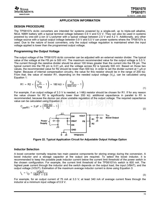
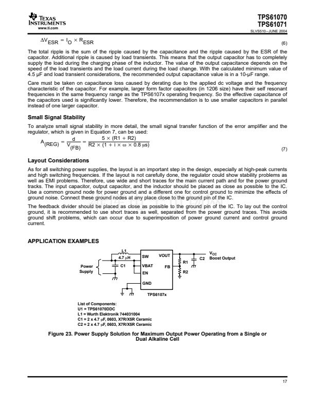
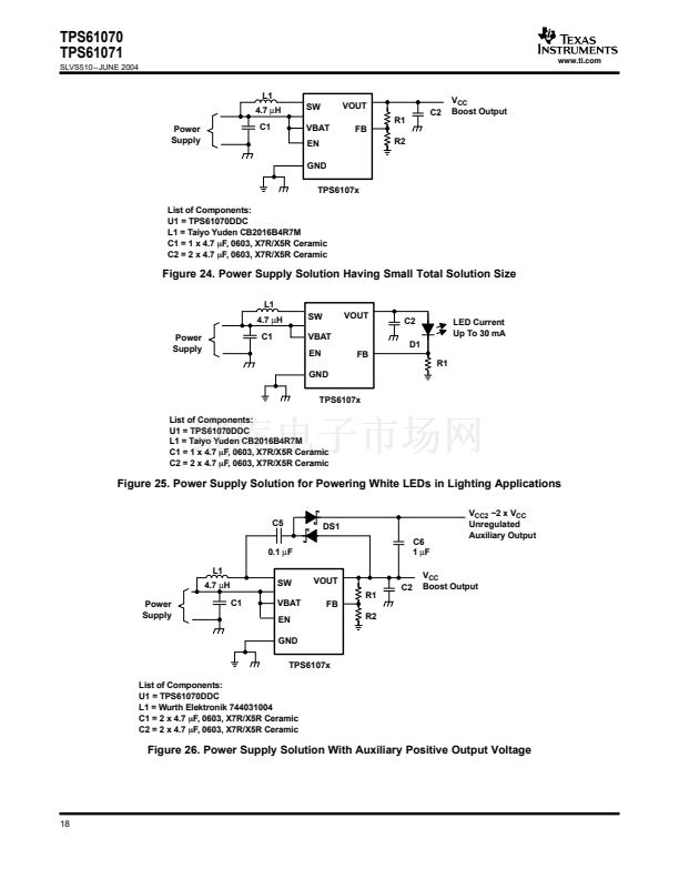
TPS61070
TPS61071
SLVS510 鈥?JUNE 2004
www.ti.com
These devices have limited built-in ESD protection. The leads should be shorted together or the device
placed in conductive foam during storage or handling to prevent electrostatic damage to the MOS gates.
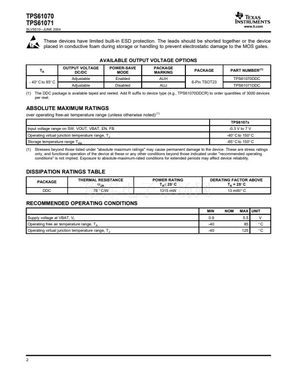
AVAILABLE OUTPUT VOLTAGE OPTIONS
T
A
- 40掳C to 85掳C
(1)
OUTPUT VOLTAGE
DC/DC
Adjustable
Adjustable
POWER-SAVE
MODE
Enabled
Disabled
PACKAGE
MARKING
AUH
AUJ
PACKAGE
6-Pin TSOT23
PART NUMBER
(1)
TPS61070DDC
TPS61071DDC
The DDC package is available taped and reeled. Add R suffix to device type (e.g., TPS61070DDCR) to order quantities of 3000 devices
per reel.
ABSOLUTE MAXIMUM RATINGS
over operating free-air temperature range (unless otherwise noted)
(1)
TPS6107x
Input voltage range on SW, VOUT, VBAT, EN, FB
Operating virtual junction temperature range, T
J
Storage temperature range T
stg
(1)
-0.3 V to 7 V
-40掳C to 150掳C
-65掳C to 150掳C
Stresses beyond those listed under "absolute maximum ratings" may cause permanent damage to the device. These are stress ratings
only, and functional operation of the device at these or any other conditions beyond those indicated under "recommended operating
conditions" is not implied. Exposure to absolute-maximum-rated conditions for extended periods may affect device reliability.
DISSIPATION RATINGS TABLE
PACKAGE
DDC
THERMAL RESISTANCE
螛
JA
76
掳C/W
POWER RATING
T
A
鈮?/div>
25掳C
1315 mW
DERATING FACTOR ABOVE
T
A
= 25掳C
13 mW/掳C
RECOMMENDED OPERATING CONDITIONS
MIN
Supply voltage at VBAT, V
I
Operating free air temperature range, T
A
Operating virtual junction temperature range, T
J
0.9
-40
-40
NOM
MAX UNIT
5.5
85
125
V
掳C
掳C
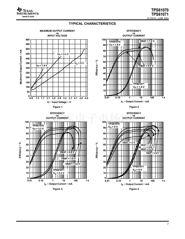
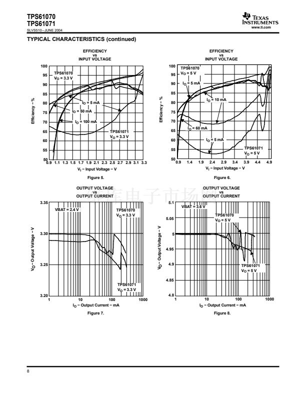
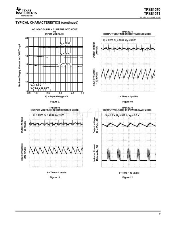
2


 1
1
 2
2
 3
3
 4
4
 5
5
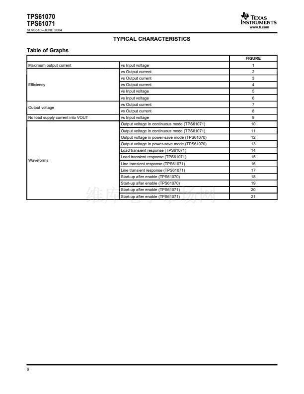 6
6
 7
7
 8
8
 9
9
 10
10
 11
11
 12
12
 13
13
 14
14
 15
15
 16
16
 17
17
 18
18
 19
19
 20
20
 21
21
