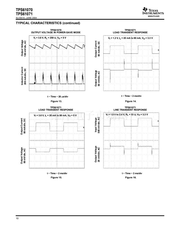
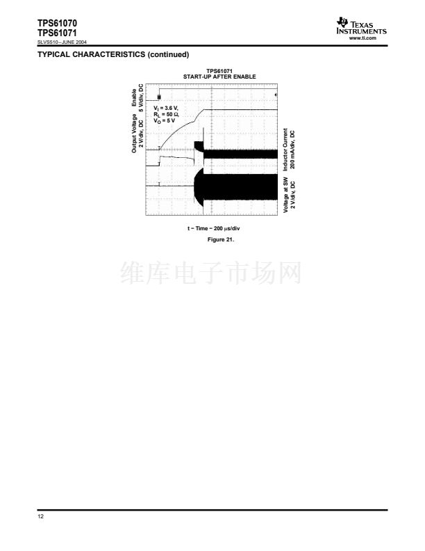
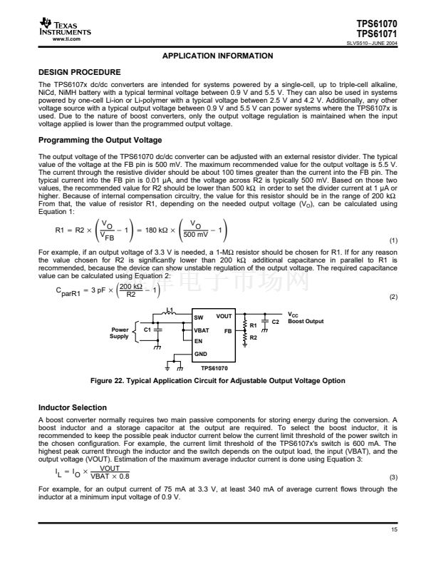
www.ti.com
TPS61070
TPS61071
SLVS510 鈥?JUNE 2004
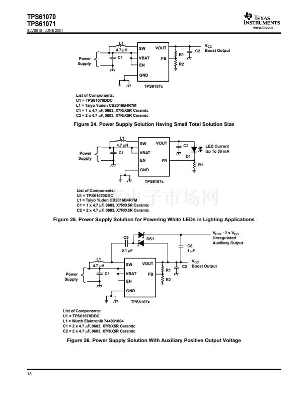
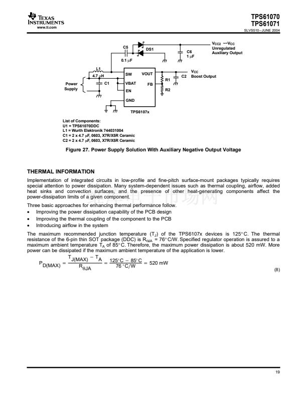
C5
0.1
碌F
L1
4.7
碌H
Power
Supply
C1
SW
VBAT
EN
GND
DS1
C6
1
碌F
V
CC2
~鈭扸
CC
Unregulated
Auxiliary Output
VOUT
R1
FB
R2
C2
V
CC
Boost Output
TPS6107x
List of Components:
U1 = TPS61070DDC
L1 = Wurth Elektronik 744031004
C1 = 2 x 4.7
mF,
0603, X7R/X5R Ceramic
C2 = 2 x 4.7
mF,
0603, X7R/X5R Ceramic
Figure 27. Power Supply Solution With Auxiliary Negative Output Voltage
THERMAL INFORMATION
Implementation of integrated circuits in low-profile and fine-pitch surface-mount packages typically requires
special attention to power dissipation. Many system-dependent issues such as thermal coupling, airflow, added
heat sinks and convection surfaces, and the presence of other heat-generating components affect the
power-dissipation limits of a given component.
Three basic approaches for enhancing thermal performance follow.
鈥?/div>
Improving the power dissipation capability of the PCB design
鈥?/div>
Improving the thermal coupling of the component to the PCB
鈥?/div>
Introducing airflow in the system
The maximum recommended junction temperature (T
J
) of the TPS6107x devices is 125掳C. The thermal
resistance of the 6-pin thin SOT package (DDC) is R
螛JA
= 76掳C/W. Specified regulator operation is assured to a
maximum ambient temperature T
A
of 85掳C. Therefore, the maximum power dissipation is about 520 mW. More
power can be dissipated if the maximum ambient temperature of the application is lower.
T
*
T
J(MAX)
A
P
+
+
125掳C
*
85掳C
+
520 mW
D(MAX)
R
76 掳C W
qJA
(8)
19


 1
1
 2
2
 3
3
 4
4
 5
5
 6
6
 7
7
 8
8
 9
9
 10
10
 11
11
 12
12
 13
13
 14
14
 15
15
 16
16
 17
17
 18
18
 19
19
 20
20
 21
21
