www.ti.com
TPS61070
TPS61071
SLVS510 鈥?JUNE 2004
DV
ESR
+
I
O
R
ESR
(6)
The total ripple is the sum of the ripple caused by the capacitance and the ripple caused by the ESR of the
capacitor. Additional ripple is caused by load transients. This means that the output capacitor has to completely
supply the load during the charging phase of the inductor. The value of the output capacitance depends on the
speed of the load transients and the load current during the load change. With the calculated minimum value of
4.5 碌F and load transient considerations, the recommended output capacitance value is in a 10-碌F range.
Care must be taken on capacitance loss caused by derating due to the applied dc voltage and the frequency
characteristic of the capacitor. For example, larger form factor capacitors (in 1206 size) have their self resonant
frequencies in the same frequency range as the TPS6107x operating frequency. So the effective capacitance of
the capacitors used is significantly lower. Therefore, the recommendation is to use smaller capacitors in parallel
instead of one larger capacitor.
Small Signal Stability
To analyze small signal stability in more detail, the small signal transfer function of the error amplifier and the
regulator, which is given in Equation 7, can be used:
5 (R1
)
R2)
A
+
d
+
(REG)
V
R2 (1
)
i
w
0.8
ms)
(FB)
(7)
Layout Considerations
As for all switching power supplies, the layout is an important step in the design, especially at high-peak currents
and high switching frequencies. If the layout is not carefully done, the regulator could show stability problems as
well as EMI problems. Therefore, use wide and short traces for the main current path and for the power ground
tracks. The input capacitor, output capacitor, and the inductor should be placed as close as possible to the IC.
Use a common ground node for power ground and a different one for control ground to minimize the effects of
ground noise. Connect these ground nodes at any place close to the ground pin of the IC.
The feedback divider should be placed as close as possible to the ground pin of the IC. To lay out the control
ground, it is recommended to use short traces as well, separated from the power ground traces. This avoids
ground shift problems, which can occur due to superimposition of power ground current and control ground
current.
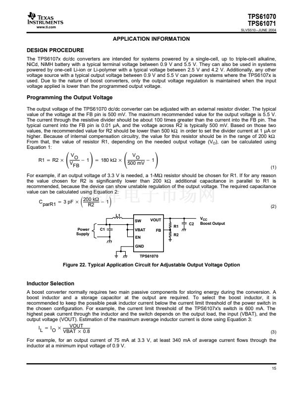
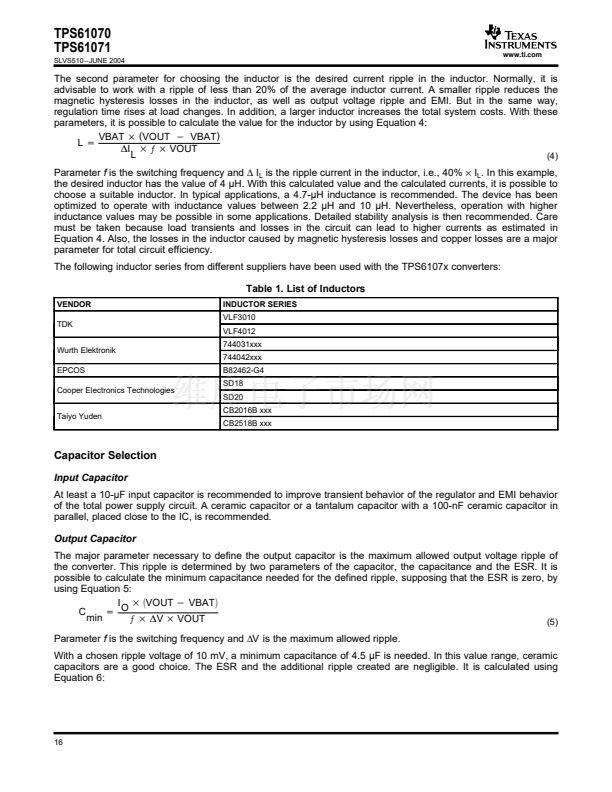
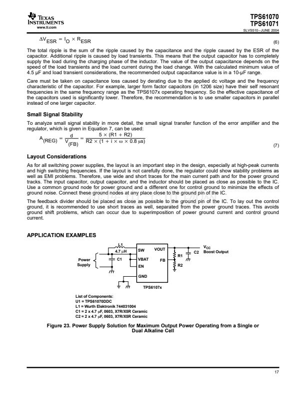
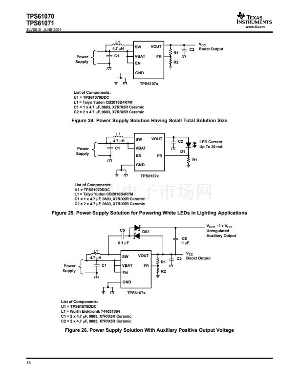
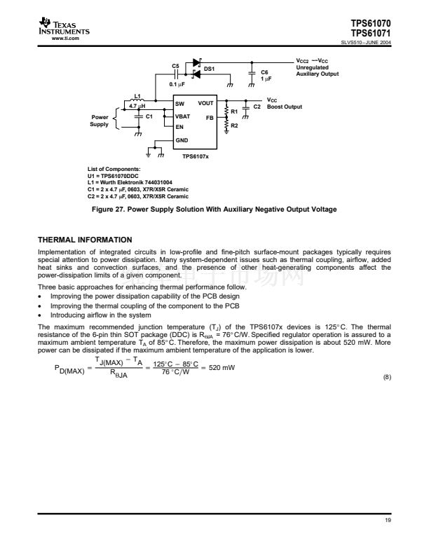
APPLICATION EXAMPLES
L1
4.7
碌H
Power
Supply
C1
SW
VBAT
EN
GND
TPS6107x
List of Components:
U1 = TPS61070DDC
L1 = Wurth Elektronik 744031004
C1 = 2 x 4.7
mF,
0603, X7R/X5R Ceramic
C2 = 2 x 4.7
mF,
0603, X7R/X5R Ceramic
VOUT
R1
FB
R2
C2
V
CC
Boost Output
Figure 23. Power Supply Solution for Maximum Output Power Operating from a Single or
Dual Alkaline Cell
17


 1
1
 2
2
 3
3
 4
4
 5
5
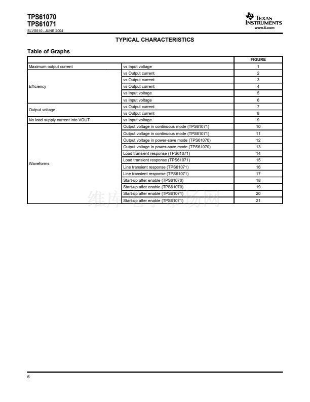 6
6
 7
7
 8
8
 9
9
 10
10
 11
11
 12
12
 13
13
 14
14
 15
15
 16
16
 17
17
 18
18
 19
19
 20
20
 21
21
