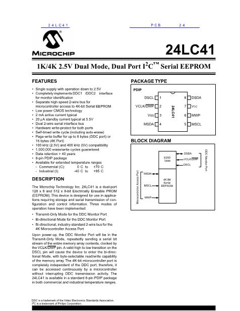
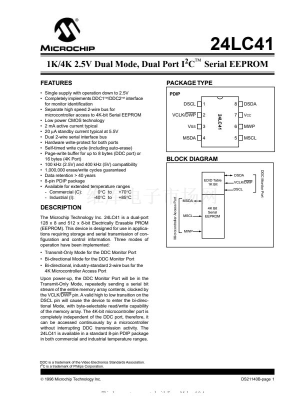
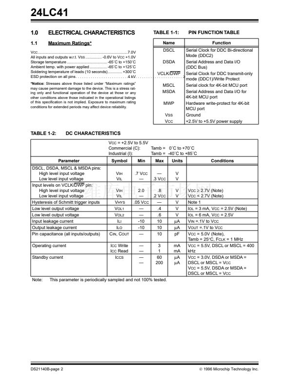
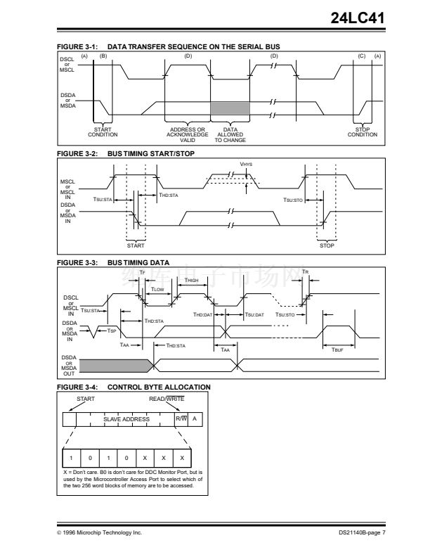
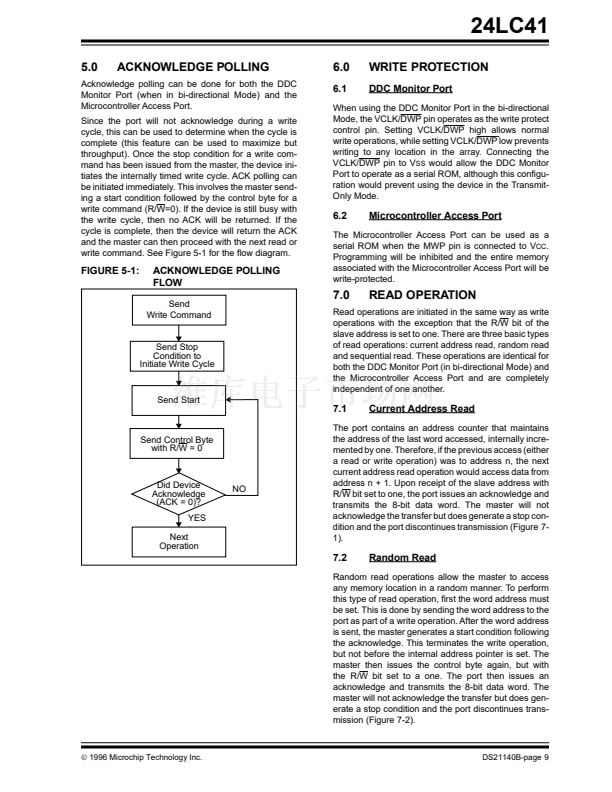
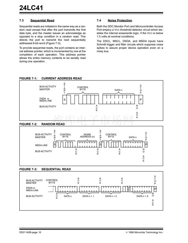
鈥?/div>
25
掳
C, Vcc = 5.0V, Block
Mode (Note 4)
Note 1: Not 100% tested. C
B
= total capacitance of one bus line in pF.
2: As a transmitter, the device must provide an internal minimum delay time to bridge the unde铿乶ed region
(minimum 300 ns) of the falling edge of DSCL or MSCL to avoid unintended generation of START or STOP
conditions.
3: The combined T
SP
and V
HYS
speci铿乧ations are due to new Schmitt trigger inputs which provide improved
noise and spike suppression. This eliminates the need for a T
I
speci铿乧ation for standard operation.
4: This parameter is not tested but guaranteed by characterization. For endurance estimates in a speci铿乧
application, please consult the Total Endurance Model which can be obtained on our BBS or website.
漏
1996 Microchip Technology Inc.
DS21140B-page 3


 1
1
 2
2
 3
3
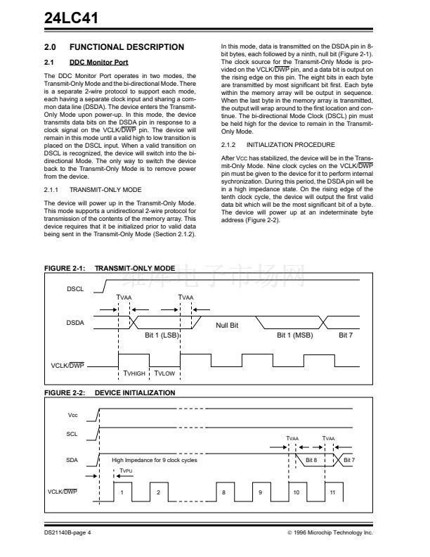 4
4
 5
5
 6
6
 7
7
 8
8
 9
9
 10
10
 11
11
 12
12
