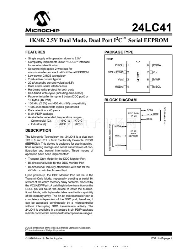
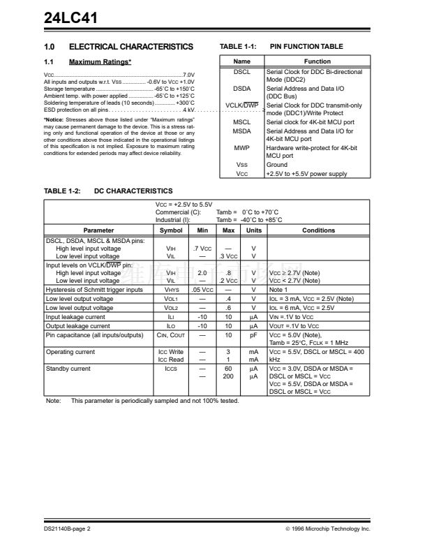
24LC41
2.0
2.1
FUNCTIONAL DESCRIPTION
DDC Monitor Port
The DDC Monitor Port operates in two modes, the
Transmit-Only Mode and the bi-directional Mode. There
is a separate 2-wire protocol to support each mode,
each having a separate clock input and sharing a com-
mon data line (DSDA). The device enters the Transmit-
Only Mode upon power-up. In this mode, the device
transmits data bits on the DSDA pin in response to a
clock signal on the VCLK/DWP pin. The device will
remain in this mode until a valid high to low transition is
placed on the DSCL input. When a valid transition on
DSCL is recognized, the device will switch into the bi-
directional Mode. The only way to switch the device
back to the Transmit-Only Mode is to remove power
from the device.
2.1.1
TRANSMIT-ONLY MODE
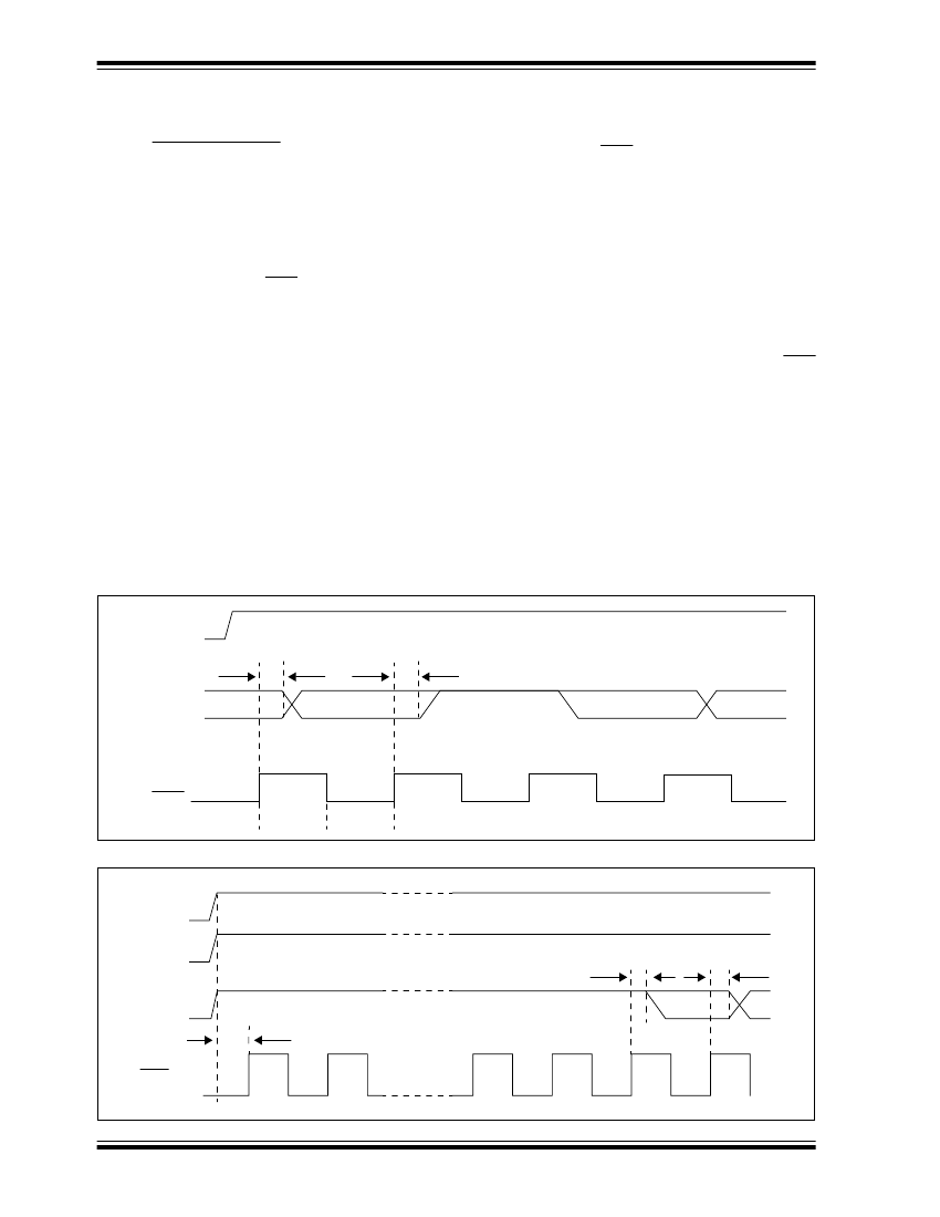
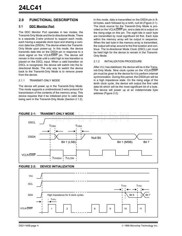
In this mode, data is transmitted on the DSDA pin in 8-
bit bytes, each followed by a ninth, null bit (Figure 2-1).
The clock source for the Transmit-Only Mode is pro-
vided on the VCLK/DWP pin, and a data bit is output on
the rising edge on this pin. The eight bits in each byte
are transmitted by most signi铿乧ant bit 铿乺st. Each byte
within the memory array will be output in sequence.
When the last byte in the memory array is transmitted,
the output will wrap around to the 铿乺st location and con-
tinue. The bi-directional Mode Clock (DSCL) pin must
be held high for the device to remain in the Transmit-
Only Mode.
2.1.2
INITIALIZATION PROCEDURE
The device will power up in the Transmit-Only Mode.
This mode supports a unidirectional 2-wire protocol for
transmission of the contents of the memory array. This
device requires that it be initialized prior to valid data
being sent in the Transmit-Only Mode (Section 2.1.2).
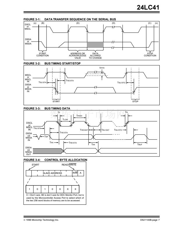
After V
CC
has stabilized, the device will be in the Trans-
mit-Only Mode. Nine clock cycles on the VCLK/DWP
pin must be given to the device for it to perform internal
sychronization. During this period, the DSDA pin will be
in a high impedance state. On the rising edge of the
tenth clock cycle, the device will output the 铿乺st valid
data bit which will be the most signi铿乧ant bit of a byte.
The device will power up at an indeterminate byte
address (Figure 2-2).
FIGURE 2-1:
DSCL
TRANSMIT-ONLY MODE
T
VAA
T
VAA
DSDA
Null Bit
Bit 1 (LSB)
Bit 1 (MSB)
Bit 7
VCLK/DWP
T
VHIGH
FIGURE 2-2:
Vcc
SCL
T
VLOW
DEVICE INITIALIZATION
T
VAA
T
VAA
SDA
High Impedance for 9 clock cycles
T
VPU
Bit 8
Bit 7
VCLK/DWP
1
2
8
9
10
11
DS21140B-page 4
漏
1996 Microchip Technology Inc.


 1
1
 2
2
 3
3
 4
4
 5
5
 6
6
 7
7
 8
8
 9
9
 10
10
 11
11
 12
12
