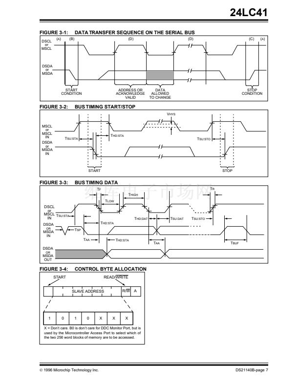
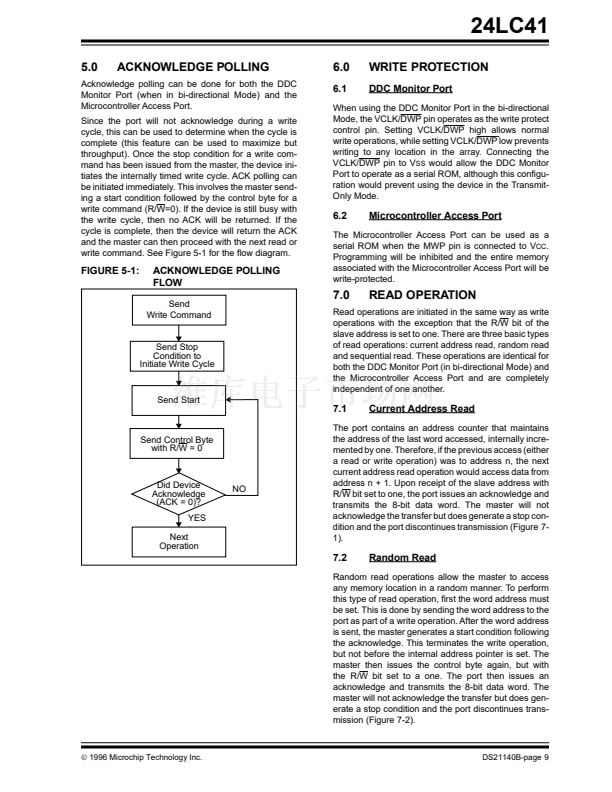
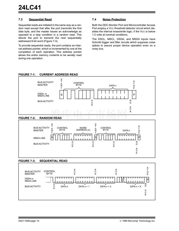
24LC41
4.0
WRITE OPERATION
Write operations are identical for the DDC Monitor Port
(when in bi-directional Mode) and the Microcontroller
Access Port, with the exception of the VCLK/DWP and
MWP pins noted in the next sections. Data can be writ-
ten using either a byte write or page write command.
Write commands for the DDC Monitor Port and the
Microcontroller Access Port are completely indepen-
dent of one another.
For the Microcontroller Access Port, the MWP pin must
be held to V
SS
during the entire write operation.
4.2
Page Write
4.1
Byte Write
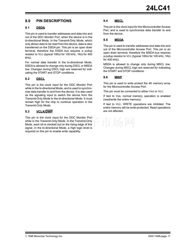
Following the start signal from the master, the slave
address (4-bits), the chip select bits (3-bits) and the
R/W bit which is a logic low is placed onto the bus by
the master transmitter. This indicates to the addressed
slave receiver that a byte with a word address will follow
after it has generated an acknowledge bit during the
ninth clock cycle. Therefore, the next byte transmitted
by the master is the word address and will be written
into the address pointer of the port. After receiving
another acknowledge signal from the port, the master
device will transmit the data word to be written into the
addressed memory location. The port acknowledges
again and the master generates a stop condition. This
initiates the internal write cycle, and during this time,
the port will not generate acknowledge signals
(Figure 4-1).
For the DDC Monitor Port it is required that VCLK/DWP
be held at a logic high level in order to program the
device. This applies to byte write and page write opera-
tion. Note that VCLK/DWP can go low while the device
is in its self-timed program operation and not affect pro-
gramming.
The write control byte, word address, and the 铿乺st data
byte are transmitted to the port in the same way as in a
byte write. But, instead of generating a stop condition,
the master transmits up to eight data bytes to the DDC
Monitor Port or 16 bytes to the Microcontroller Access
Port, which are temporarily stored in the on-chip page
buffer and will be written into the memory after the mas-
ter has transmitted a stop condition. After the receipt of
each word, the three lower order address pointer bits
are internally incremented by one. The higher order 5-
bits of the word address remains constant. If the master
should transmit more than eight words to the DDC Mon-
itor Port or 16 words to the Microcontroller Access Port
prior to generating the stop condition, the address
counter will roll over and the previously received data
will be overwritten. As with the byte write operation,
once the stop condition is received an internal write
cycle will begin (Figure 4-2).
For the DDC Monitor Port, it is required thatVCLK/DWP
be held at a logic high level in order to program the
device. This applies to byte write and page write opera-
tion. Note that VCLK/DWP can go low while the device
is in its self-timed program operation and not affect pro-
gramming.
For the Microcontroller Access Port, the MWP pin must
be held to V
SS
during the entire write operation.
FIGURE 4-1:
BUS ACTIVITY
MASTER
BYTE WRITE
S
T
A
R
T
CONTROL
BYTE
WORD
ADDRESS
DATA
S
T
O
P
SDA or
MSDA LINE
S
A
C
K
A
C
K
A
C
K
P
BUS ACTIVITY
VCLK
FIGURE 4-2:
BUS ACTIVITY
MASTER
PAGE WRITE
S
T
A
R
T
S
T
O
P
CONTROL
BYTE
WORD
ADDRESS (n)
DATA n
DATA n + 1
DATA n + 15
SDA LINE
BUS ACTIVITY
S
A
C
K
A
C
K
A
C
K
A
C
K
A
C
K
P
VCLK/DWP
DS21140B-page 8
漏
1996 Microchip Technology Inc.


 1
1
 2
2
 3
3
 4
4
 5
5
 6
6
 7
7
 8
8
 9
9
 10
10
 11
11
 12
12
