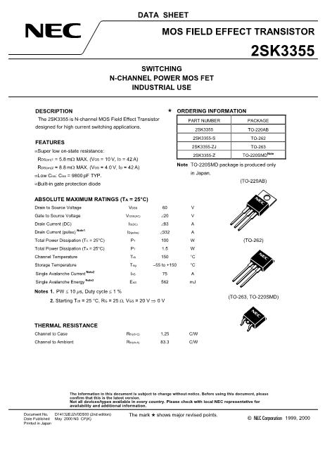
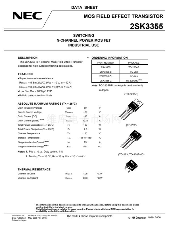
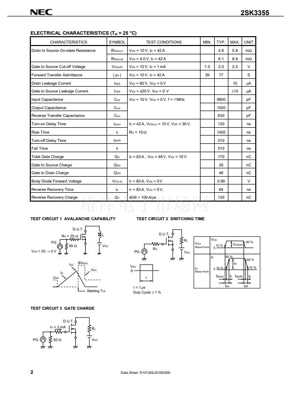
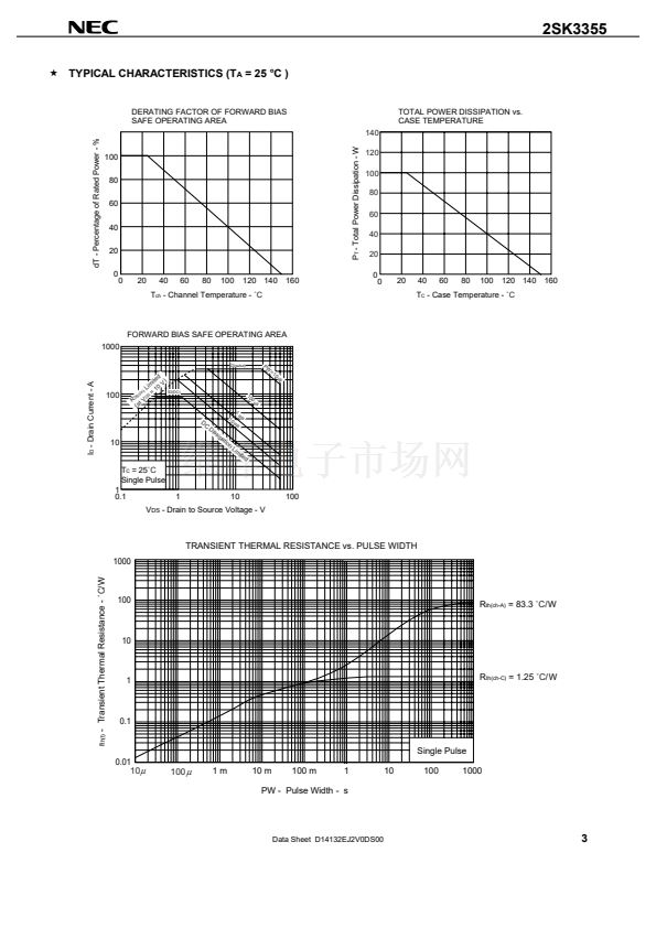
2SK3355
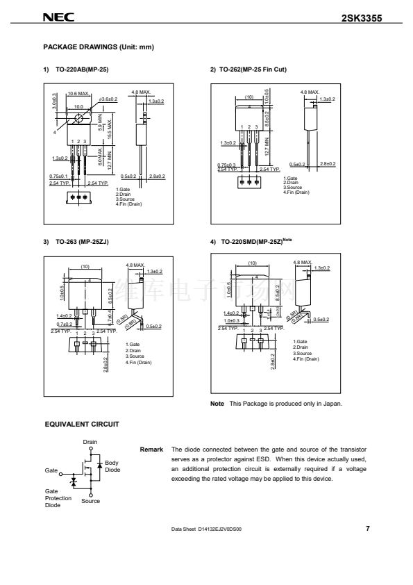
PACKAGE DRAWINGS (Unit: mm)
1)
TO-220AB(MP-25)
2) TO-262(MP-25 Fin Cut)
3.0卤0.3
10.6 MAX.
10.0
4.8 MAX.
1.0卤0.5
4.8 MAX.
1.3卤0.2
蠁
3.6卤0.2
5.9 MIN.
(10)
1.3卤0.2
4
15.5 MAX.
1
2
3
4
1 2 3
6.0 MAX.
1.3卤0.2
12.7 MIN.
1.3卤0.2
12.7 MIN.
8.5卤0.2
0.75卤0.3
2.54 TYP.
0.5卤0.2
2.54 TYP.
1.Gate
2.Drain
3.Source
4.Fin (Drain)
2.8卤0.2
0.75卤0.1
2.54 TYP.
0.5卤0.2
2.54 TYP.
1.Gate
2.Drain
3.Source
4.Fin (Drain)
2.8卤0.2
3)
TO-263 (MP-25ZJ)
4) TO-220SMD(MP-25Z)
Note
(10)
4
1.0卤0.5
8.5卤0.2
4.8 MAX.
1.3卤0.2
(10)
4
4.8 MAX.
1.3卤0.2
1.0卤0.5
5.7卤0.4
11卤0.4
3.0卤0.5
8.5卤0.2
R)
)
0.5
.8R
(
(0
1.4卤0.2
0.7卤0.2
2.54 TYP. 1
2
(0
)
.5R
1.4卤0.2
)
3 2.54 TYP.
.8R
(0
1.0卤0.3
0.5卤0.2
2.54 TYP. 1
2
0.5卤0.2
3 2.54 TYP.
1.Gate
2.Drain
3.Source
4.Fin (Drain)
2.8卤0.2
Note
This Package is produced only in Japan.
EQUIVALENT CIRCUIT
Drain
Remark
Gate
Body
Diode
The diode connected between the gate and source of the transistor
serves as a protector against ESD. When this device actually used,
an additional protection circuit is externally required if a voltage
exceeding the rated voltage may be applied to this device.
Gate
Protection
Diode
Source
2.8卤0.2
1.Gate
2.Drain
3.Source
4.Fin (Drain)
Data Sheet D14132EJ2V0DS00
7


 1
1
 2
2
 3
3
 4
4
 5
5
 6
6
 7
7
 8
8
