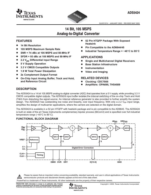
ADS5424
www.ti.com
SLWS157A 鈭?JANUARY 2005 鈭?REVISED MAY 2005
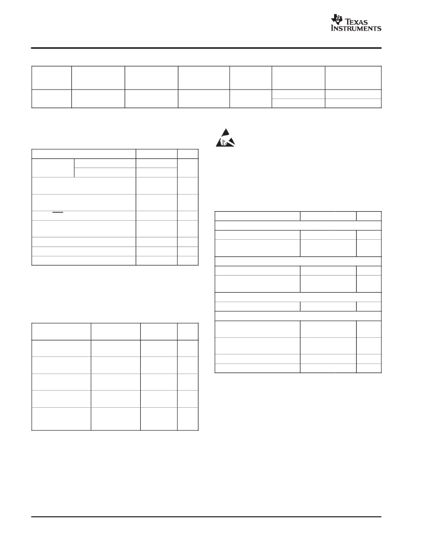
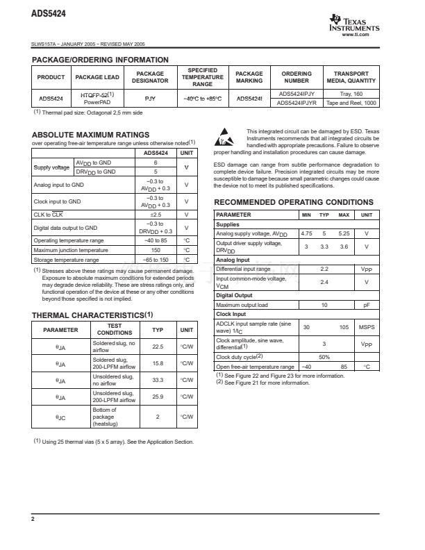
PACKAGE/ORDERING INFORMATION
PRODUCT
PACKAGE LEAD
HTQFP-52(1)
PowerPAD
PACKAGE
DESIGNATOR
PJY
SPECIFIED
TEMPERATURE
RANGE
鈭?0掳C to +85掳C
PACKAGE
MARKING
ADS5424I
ORDERING
NUMBER
ADS5424IPJY
ADS5424IPJYR
TRANSPORT
MEDIA, QUANTITY
Tray, 160
Tape and Reel, 1000
ADS5424
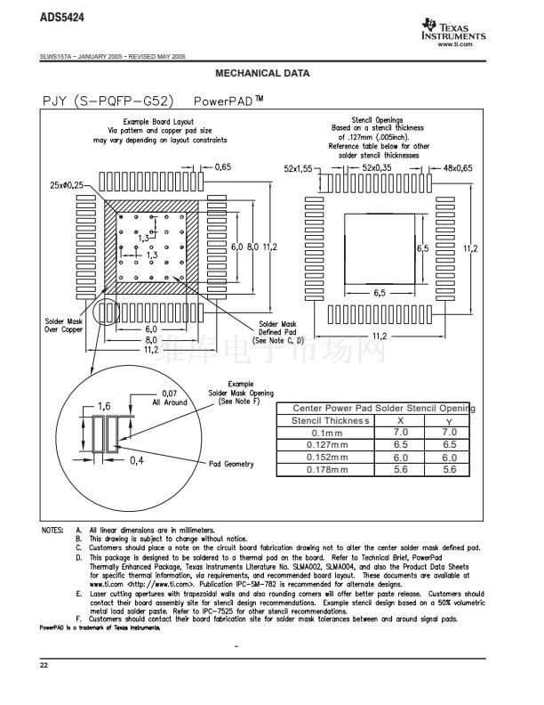
(1) Thermal pad size: Octagonal 2,5 mm side
ABSOLUTE MAXIMUM RATINGS
over operating free-air temperature range unless otherwise noted(1)
ADS5424
Supply voltage
AVDD to GND
DRVDD to GND
6
5
鈭?.3 to
AVDD + 0.3
鈭?.3 to
AVDD + 0.3
卤2.5
鈭?.3 to
DRVDD + 0.3
鈭?0 to 85
150
鈭?5 to 150
V
V
V
V
V
掳C
掳C
掳C
UNIT
This integrated circuit can be damaged by ESD. Texas
Instruments recommends that all integrated circuits be
handled with appropriate precautions. Failure to observe
proper handling and installation procedures can cause damage.
ESD damage can range from subtle performance degradation to
complete device failure. Precision integrated circuits may be more
susceptible to damage because small parametric changes could cause
the device not to meet its published specifications.
Analog input to GND
Clock input to GND
CLK to CLK
Digital data output to GND
Operating temperature range
Maximum junction temperature
Storage temperature range
RECOMMENDED OPERATING CONDITIONS
PARAMETER
Supplies
Analog supply voltage, AVDD
Output driver supply voltage,
DRVDD
Analog Input
Differential input range
Input common-mode voltage,
VCM
Digital Output
Maximum output load
10
pF
Clock Input
2.2
2.4
VPP
V
4.75
3
5
3.3
5.25
3.6
V
V
MIN
TYP
MAX
UNIT
(1) Stresses above these ratings may cause permanent damage.
Exposure to absolute maximum conditions for extended periods
may degrade device reliability. These are stress ratings only, and
functional operation of the device at these or any other conditions
beyond those specified is not implied.
THERMAL CHARACTERISTICS
(1)
PARAMETER
胃
JA
胃
JA
胃
JA
胃
JA
胃
JC
TEST
CONDITIONS
Soldered slug, no
airflow
Soldered slug,
200-LPFM airflow
Unsoldered slug,
no airflow
Unsoldered slug,
200-LPFM airflow
Bottom of
package
(heatslug)
TYP
22.5
15.8
33.3
25.9
UNIT
掳C/W
掳C/W
掳C/W
掳C/W
掳C/W
ADCLK input sample rate (sine
wave) 1/tC
Clock amplitude, sine wave,
differential(1)
Clock duty cycle(2)
30
3
50%
105
MSPS
VPP
Open free-air temperature range 鈭?0
85
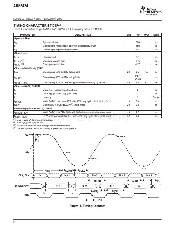
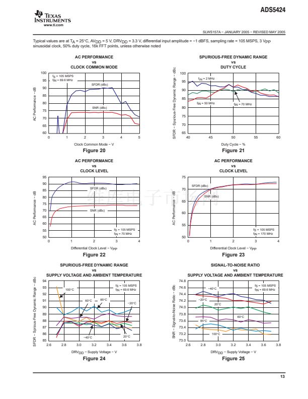
(1) See Figure 22 and Figure 23 for more information.
(2) See Figure 21 for more information.
掳C
2
(1) Using 25 thermal vias (5 x 5 array). See the Application Section.
2


 1
1
 2
2
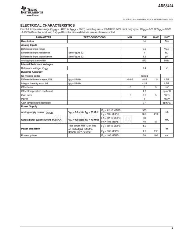 3
3
 4
4
 5
5
 6
6
 7
7
 8
8
 9
9
 10
10
 11
11
 12
12
 13
13
 14
14
 15
15
 16
16
 17
17
 18
18
 19
19
 20
20
 21
21
 22
22
 23
23
 24
24
 25
25
