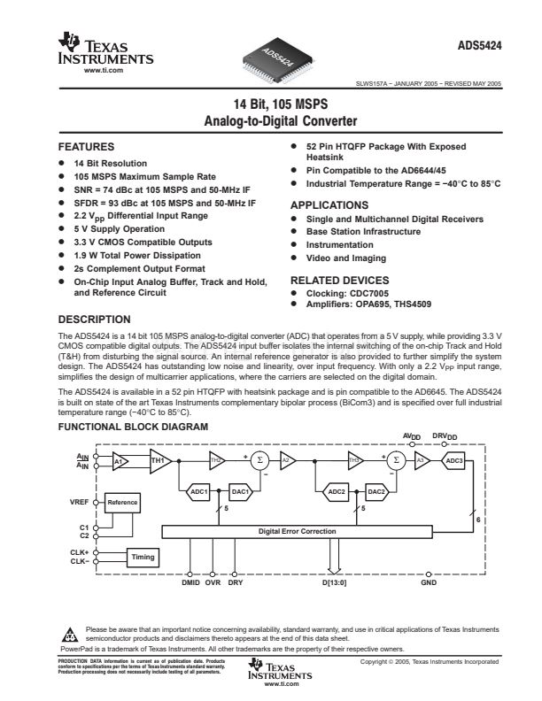
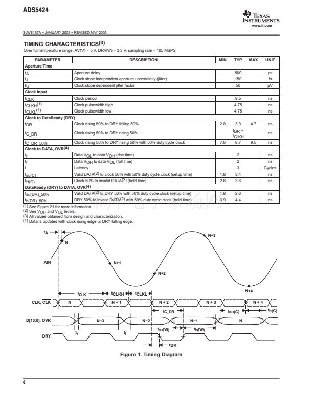
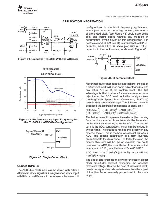
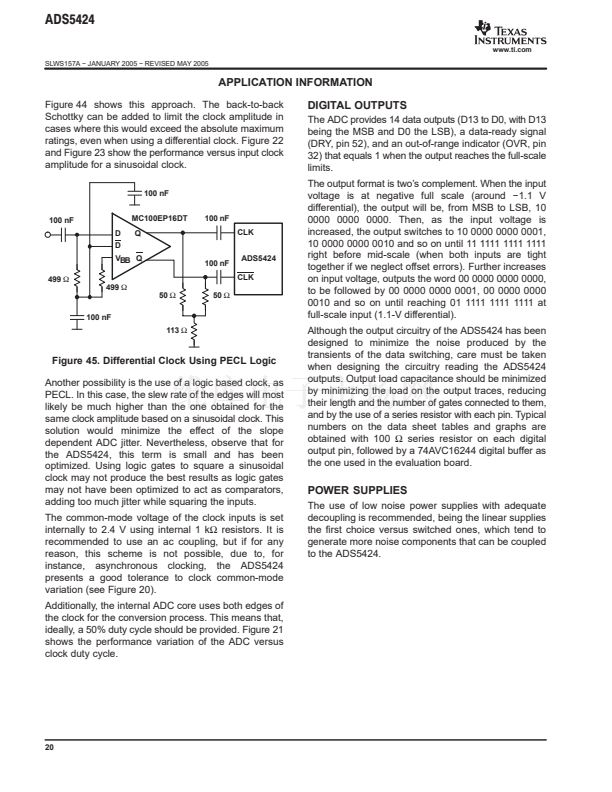
ADS5424
www.ti.com
SLWS157A 鈭?JANUARY 2005 鈭?REVISED MAY 2005
TIMING CHARACTERISTICS
(3)
Over full temperature range, AVDD = 5 V, DRVDD = 3.3 V, sampling rate = 105 MSPS
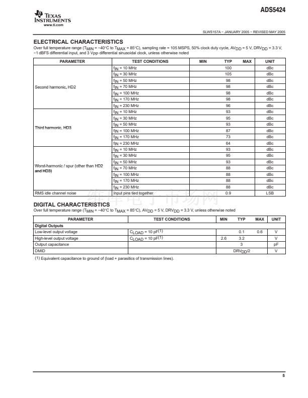
PARAMETER
Aperture Time
tA
tJ
kJ
Clock Input
tCLK
tCLKH(1)
tCLKL(1)
tDR
tC_DR
tC_DR_50%
Clock to DATA, OVR(4)
tr
tf
L
tsu(C)
tH(C)
Clock period
Clock pulsewidth high
Clock pulsewidth low
Clock rising 50% to DRY falling 50%
Clock rising 50% to DRY rising 50%
Clock rising 50% to DRY rising 50% with 50% duty cycle clock
Data VOL to data VOH (rise time)
Data VOH to data VOL (fall time)
Latency
Valid DATA(2) to clock 50% with 50% duty cycle clock (setup time)
Clock 50% to invalid DATA(2) (hold time)
1.8
2.6
1.8
3.9
7.6
2.8
9.5
4.75
4.75
3.9
tDR +
tCLKH
8.7
2
2
3
3.4
3.6
2.6
4.4
4.7
ns
ns
ns
ns
ns
9.5
ns
ns
ns
Cycles
ns
ns
ns
ns
Aperture delay
Clock slope independent aperture uncertainity (jitter)
Clock slope dependent jitter factor
500
150
50
ps
fs
碌V
DESCRIPTION
MIN
TYP
MAX
UNIT
Clock to DataReady (DRY)
DataReady (DRY) to DATA, OVR(4)
tsu(DR)_50%
Valid DATA(2) to DRY 50% with 50% duty cycle clock (setup time)
th(DR)_50%
DRY 50% to invalid DATA(2) with 50% duty cycle clock (hold time)
(1) See Figure 21 for more information.
(2)
See VOH and VOL levels.
(3) All values obtained from design and characterization.
(4) Data is updated with clock rising edge or DRY falling edge.
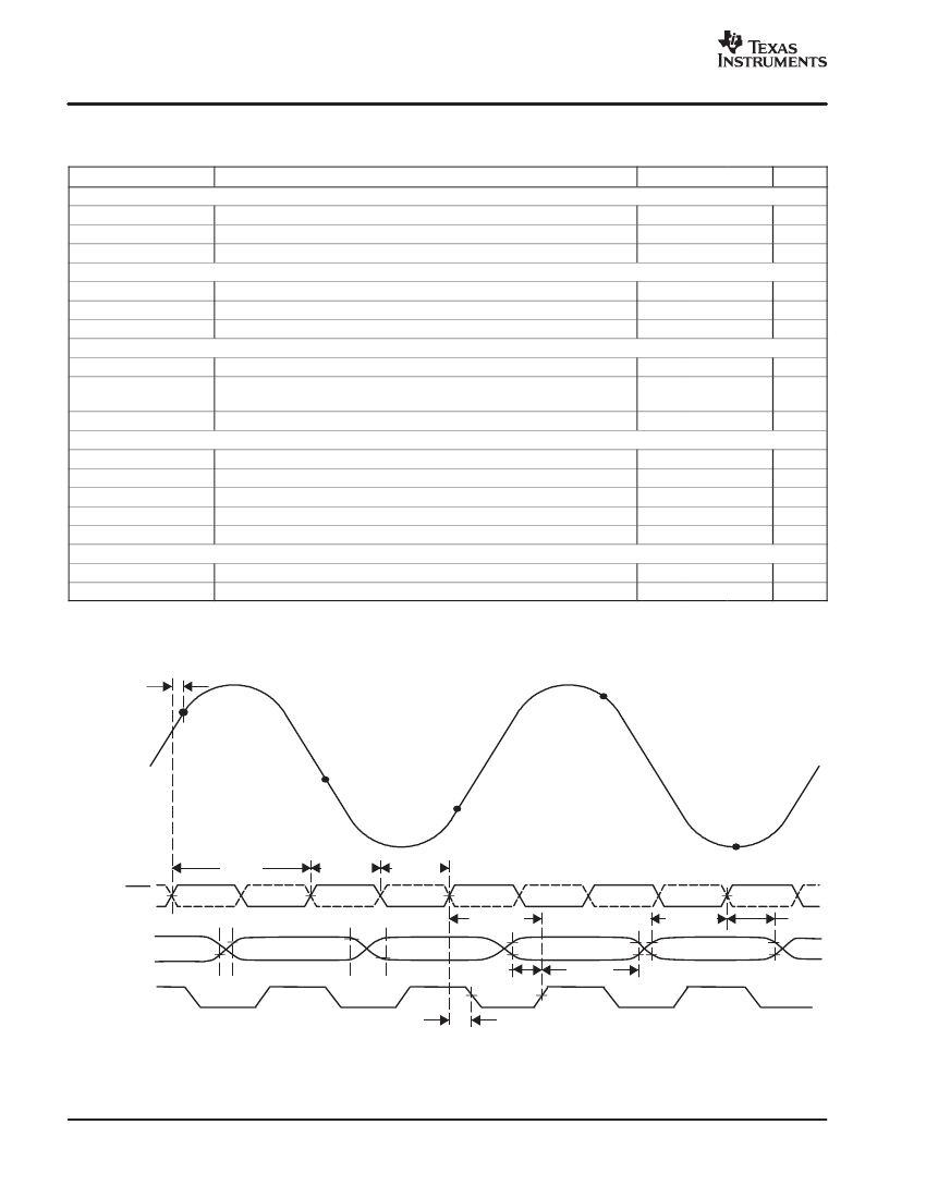
tA
N
N+3
AIN
N+1
N+2
tCLK
CLK, CLK
N
tCLKH
N+1
tCLKL
N+2
tC_DR
N+3
tsu(C)
N鈭?
tsu(DR)
th(DR)
N
N+4
N+4
th(C)
D[13:0], OVR
tr
N鈭?
tf
N鈭?
DRY
tDR
Figure 1. Timing Diagram
6


 1
1
 2
2
 3
3
 4
4
 5
5
 6
6
 7
7
 8
8
 9
9
 10
10
 11
11
 12
12
 13
13
 14
14
 15
15
 16
16
 17
17
 18
18
 19
19
 20
20
 21
21
 22
22
 23
23
 24
24
 25
25
