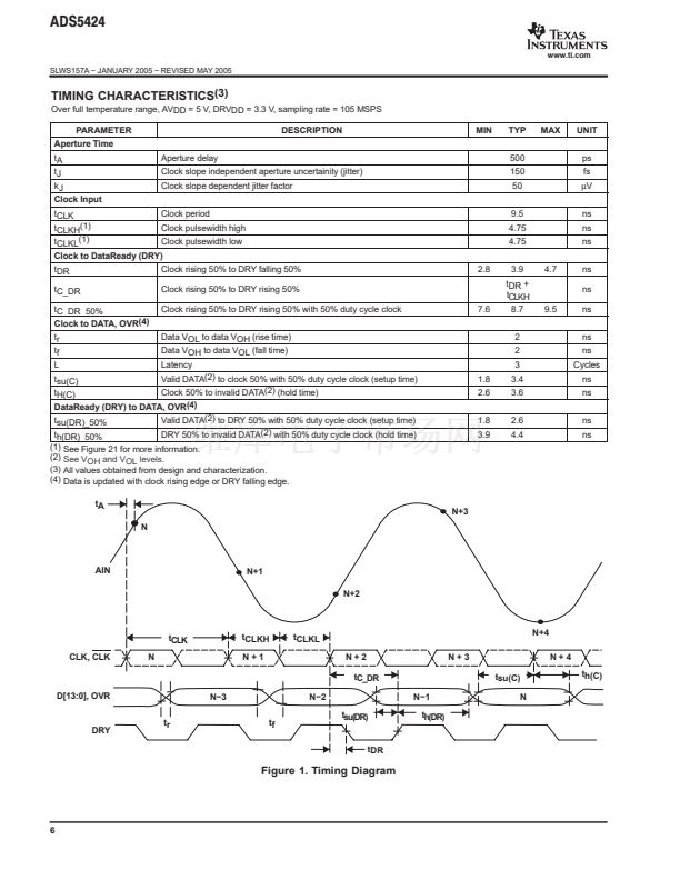
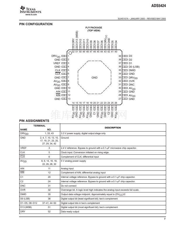
ADS5424
www.ti.com
SLWS157A 鈭?JANUARY 2005 鈭?REVISED MAY 2005
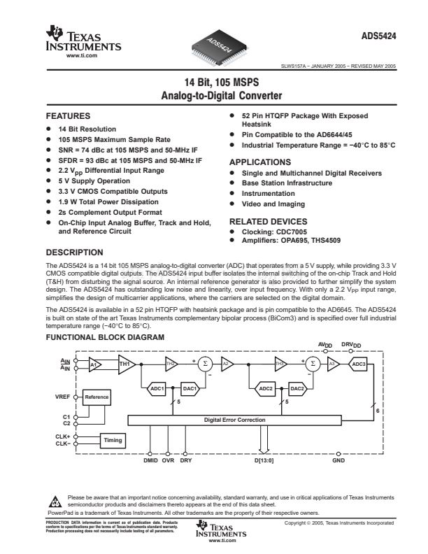
APPLICATION INFORMATION
The ADS5424 uses two power supplies. For the analog
portion of the design, a 5 V AV
DD
is used, while for the
digital outputs supply (DRV
DD
), we recommend the use
of 3.3 V. All the ground pins are marked as GND,
although AGND pins and DRGND pins are not tied
together inside the package. Customers willing to
experiment with different grounding schemes should
know that AGND pins are 4, 7, 10, 13, 15, 17, 19, 21,
23, 25, 27, and 29, while DRGND pins are 2, 34, and 42.
Nevertheless, we recommend that both grounds are
tied together externally, using a common ground plane.
That is the case on the production test boards and
modules provided to customer for evaluation. In order
to obtain the best performance, user should layout the
board to guarantee that the digital return currents do not
flow under the analog portion of the board. This can be
achieved without the need to split the board and just
with careful component placing and increasing the
number of vias and ground planes.
Finally, notice that the metallic heat sink under the
package is also connected to analog ground.
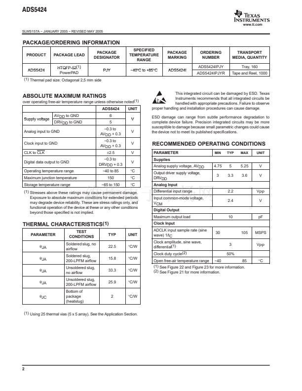
LAYOUT INFORMATION
The evaluation board represents a good guideline of
how to layout the board to obtain the maximum
performance out of the ADS5424. General design rules
as the use of multilayer boards, single ground plane for
both, analog and digital ADC ground connections and
local decoupling ceramic chip capacitors should be
applied. The input traces should be isolated from any
external source of interference or noise, including the
digital outputs as well as the clock traces. Clock should
also be isolated from other signals, especially on
applications where low jitter is required, as high IF
sampling.
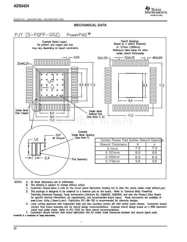
Besides performance oriented rules, special care has
to be taken when considering the heat dissipation out
of the device. The thermal heat sink (octagonal, with
2,5 mm on each side) should be soldered to the board,
and provision for more than 16 ground vias should be
made. The thermal package information describes the
T
JA
values obtained on the different configurations.
21


 1
1
 2
2
 3
3
 4
4
 5
5
 6
6
 7
7
 8
8
 9
9
 10
10
 11
11
 12
12
 13
13
 14
14
 15
15
 16
16
 17
17
 18
18
 19
19
 20
20
 21
21
 22
22
 23
23
 24
24
 25
25
