ADS5424
www.ti.com
SLWS157A 鈭?JANUARY 2005 鈭?REVISED MAY 2005
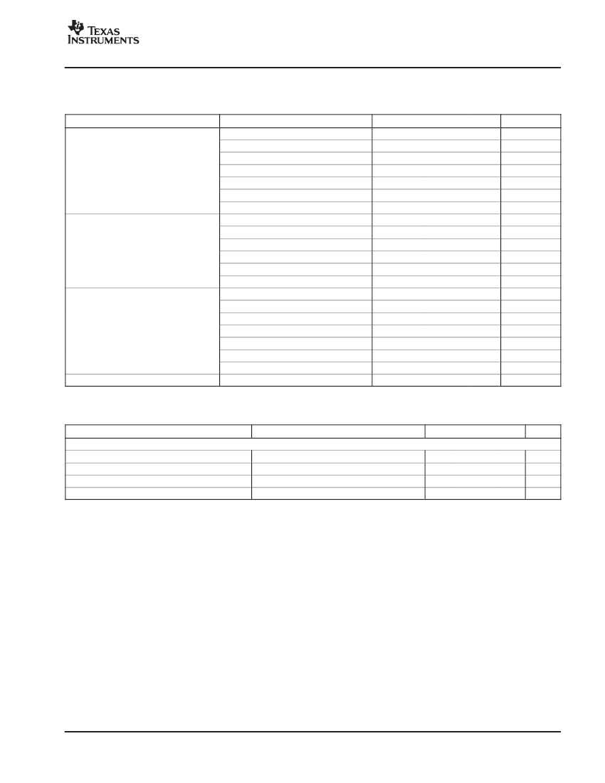
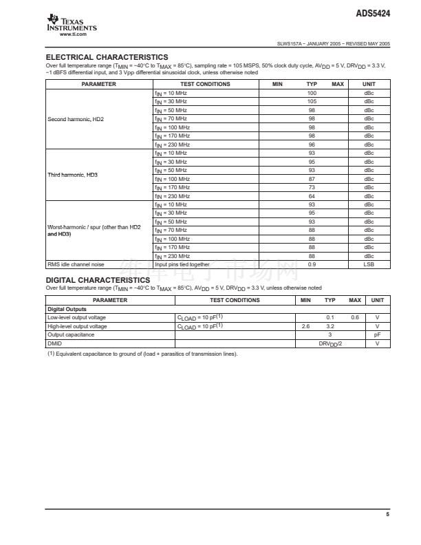
ELECTRICAL CHARACTERISTICS
Over full temperature range (TMIN = 鈭?0掳C to TMAX = 85掳C), sampling rate = 105 MSPS, 50% clock duty cycle, AVDD = 5 V, DRVDD = 3.3 V,
鈭? dBFS differential input, and 3 VPP differential sinusoidal clock, unless otherwise noted
PARAMETER
TEST CONDITIONS
fIN = 10 MHz
fIN = 30 MHz
Second harmonic, HD2
fIN = 50 MHz
fIN = 70 MHz
fIN = 100 MHz
fIN = 170 MHz
fIN = 230 MHz
fIN = 10 MHz
fIN = 30 MHz
fIN = 50 MHz
fIN = 100 MHz
fIN = 170 MHz
fIN = 230 MHz
fIN = 10 MHz
fIN = 30 MHz
fIN = 50 MHz
fIN = 70 MHz
fIN = 100 MHz
fIN = 170 MHz
fIN = 230 MHz
RMS idle channel noise
Input pins tied together
MIN
TYP
100
105
98
98
98
98
96
93
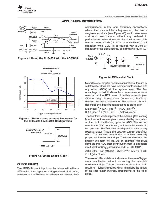
95
93
87
73
64
93
95
93
88
88
88
88
0.9
MAX
UNIT
dBc
dBc
dBc
dBc
dBc
dBc
dBc
dBc
dBc
dBc
dBc
dBc
dBc
dBc
dBc
dBc
dBc
dBc
dBc
dBc
LSB
Third harmonic, HD3
Worst-harmonic / spur (other than HD2
and HD3)
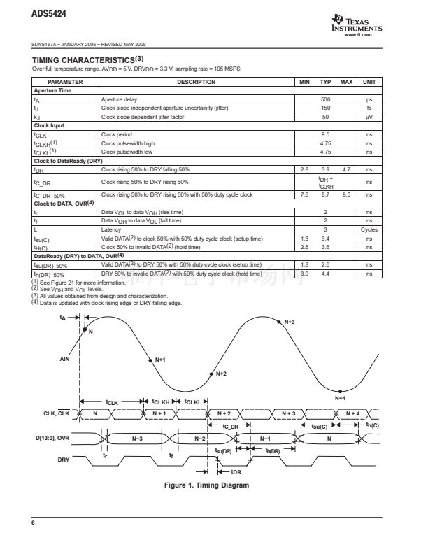
DIGITAL CHARACTERISTICS
Over full temperature range (TMIN = 鈭?0掳C to TMAX = 85掳C), AVDD = 5 V, DRVDD = 3.3 V, unless otherwise noted
PARAMETER
Digital Outputs
Low-level output voltage
High-level output voltage
Output capacitance
DMID
(1) Equivalent capacitance to ground of (load + parasitics of transmission lines).
CLOAD = 10 pF(1)
CLOAD = 10 pF(1)
0.1
2.6
3.2
3
DRVDD/2
0.6
V
V
pF
V
TEST CONDITIONS
MIN
TYP
MAX
UNIT
5


 1
1
 2
2
 3
3
 4
4
 5
5
 6
6
 7
7
 8
8
 9
9
 10
10
 11
11
 12
12
 13
13
 14
14
 15
15
 16
16
 17
17
 18
18
 19
19
 20
20
 21
21
 22
22
 23
23
 24
24
 25
25
