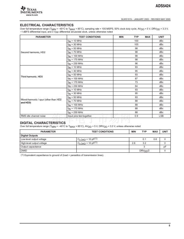
ADS5424
www.ti.com
SLWS157A 鈭?JANUARY 2005 鈭?REVISED MAY 2005
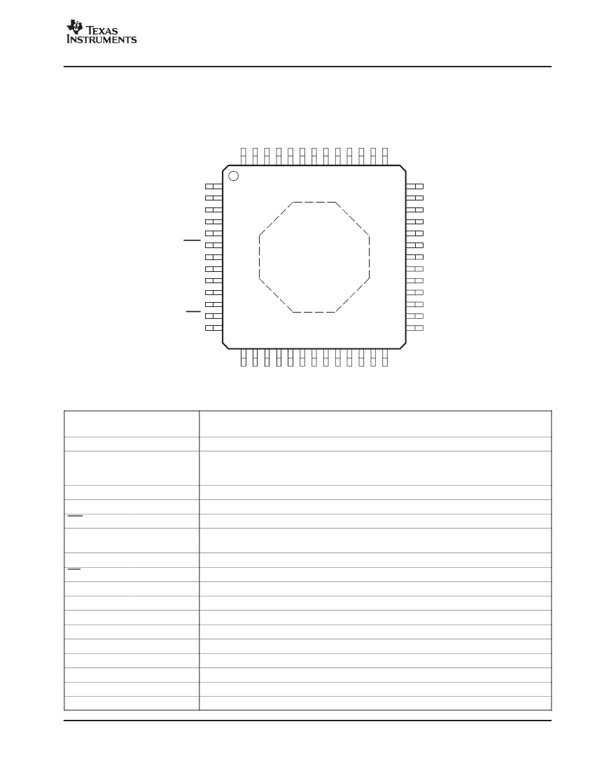
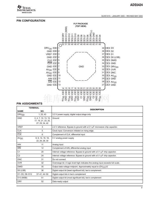
PIN CONFIGURATION
DRY
D13 (MSB)
D12
D11
D10
D9
D8
D7
D6
DRV
CC
GND
D5
D4
52 51 50 49 48 47 46 45 44 43 42 41 40
PJY PACKAGE
(TOP VIEW)
DRV
DD
GND
VREF
GND
CLK
CLK
GND
AV
DD
AV
DD
GND
AIN
AIN
GND
1
2
3
4
5
6
7
8
9
10
11
12
13
14 15 16 17 18 19 20 21 22 23 24 25 26
39
38
37
36
35
34
GND
33
32
31
30
29
28
27
D3
D2
D1
D0 (LSB)
DMID
GND
DRV
DD
OVR
DNC
AV
DD
GND
AV
DD
GND
PIN ASSIGNMENTS
TERMINAL
NAME
DRVDD
GND
NO.
1, 33, 43
2, 4, 7, 10, 13, 15,
17, 19, 21, 23, 25,
27, 29, 34, 42
3
5
6
8, 9, 14, 16, 18,
22, 26, 28, 30
11
12
20
24
31
32
35
36
37鈭?1, 44鈭?0
51
52
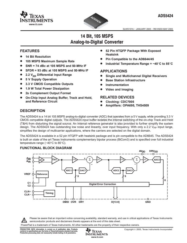
DESCRIPTION
3.3 V power supply, digital output stage only
Ground
VREF
CLK
CLK
AVDD
AIN
AIN
C1
C2
DNC
OVR
DMID
D0 (LSB)
D1鈭扗5, D6鈭扗12
D13 (MSB)
DRY
2.4 V reference. Bypass to ground with a 0.1-碌F microwave chip capacitor.
Clock input. Conversion initiated on rising edge.
Complement of CLK, differential input
5 V analog power supply
Analog input
Complement of AIN, differential analog input
Internal voltage reference. Bypass to ground with a 0.1-碌F chip capacitor.
Internal voltage reference. Bypass to ground with a 0.1-碌F chip capacitor.
Do not connect
Overrange bit. A logic level high indicates the analog input exceeds full scale.
Output data voltage midpoint. Approximately equal to (DVCC)/2
Digital output bit (least significant bit); two鈥檚 complement
Digital output bits in two鈥檚 complement
Digital output bit (most significant bit); two鈥檚 complement
Data ready output
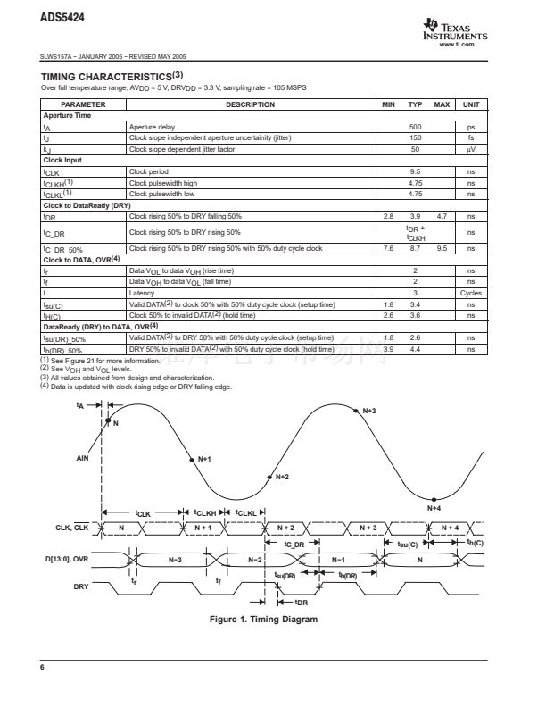
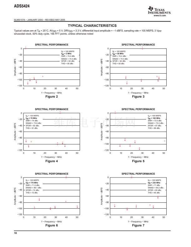
7
AV
DD
GND
AV
DD
GND
AV
DD
GND
C1
GND
AV
DD
GND
C2
GND
AV
DD


 1
1
 2
2
 3
3
 4
4
 5
5
 6
6
 7
7
 8
8
 9
9
 10
10
 11
11
 12
12
 13
13
 14
14
 15
15
 16
16
 17
17
 18
18
 19
19
 20
20
 21
21
 22
22
 23
23
 24
24
 25
25
