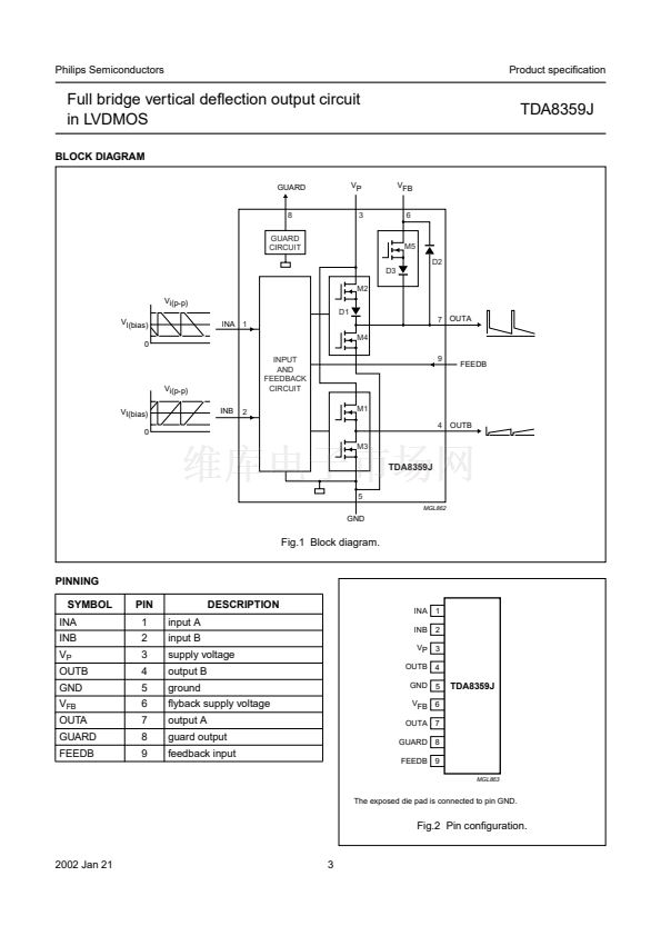
鈥?/div>
p
)
Supply voltage calculation
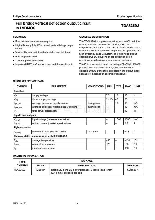
TDA8359J
For calculating the minimum required supply voltage,
several specific application parameter values have to be
known. These parameters are the required maximum
(peak) deflection coil current I
coil(peak)
, the coil impedance
R
coil
and L
coil
, and the measuring resistance of R
M
. The
required maximum (peak) deflection coil current should
also include overscan.
The deflection coil resistance has to be multiplied by 1.2 in
order to take account of hot conditions.
Chapter 鈥淐haracteristics鈥?supplies values for voltage
losses of the vertical output stage. For the first part of the
scan, the voltage loss is given by V
loss(1)
. For the second
part of the scan, the voltage loss is given by V
loss(2)
.
The voltage drop across the deflection coil during scan is
determined by the coil impedance. For the first part of the
scan the inductive contribution and the ohmic contribution
to the total coil voltage drop are of opposite sign, while for
the second part of the scan the inductive part and the
ohmic part have the same sign.
For the vertical frequency the maximum frequency
occurring must be applied to the calculations.
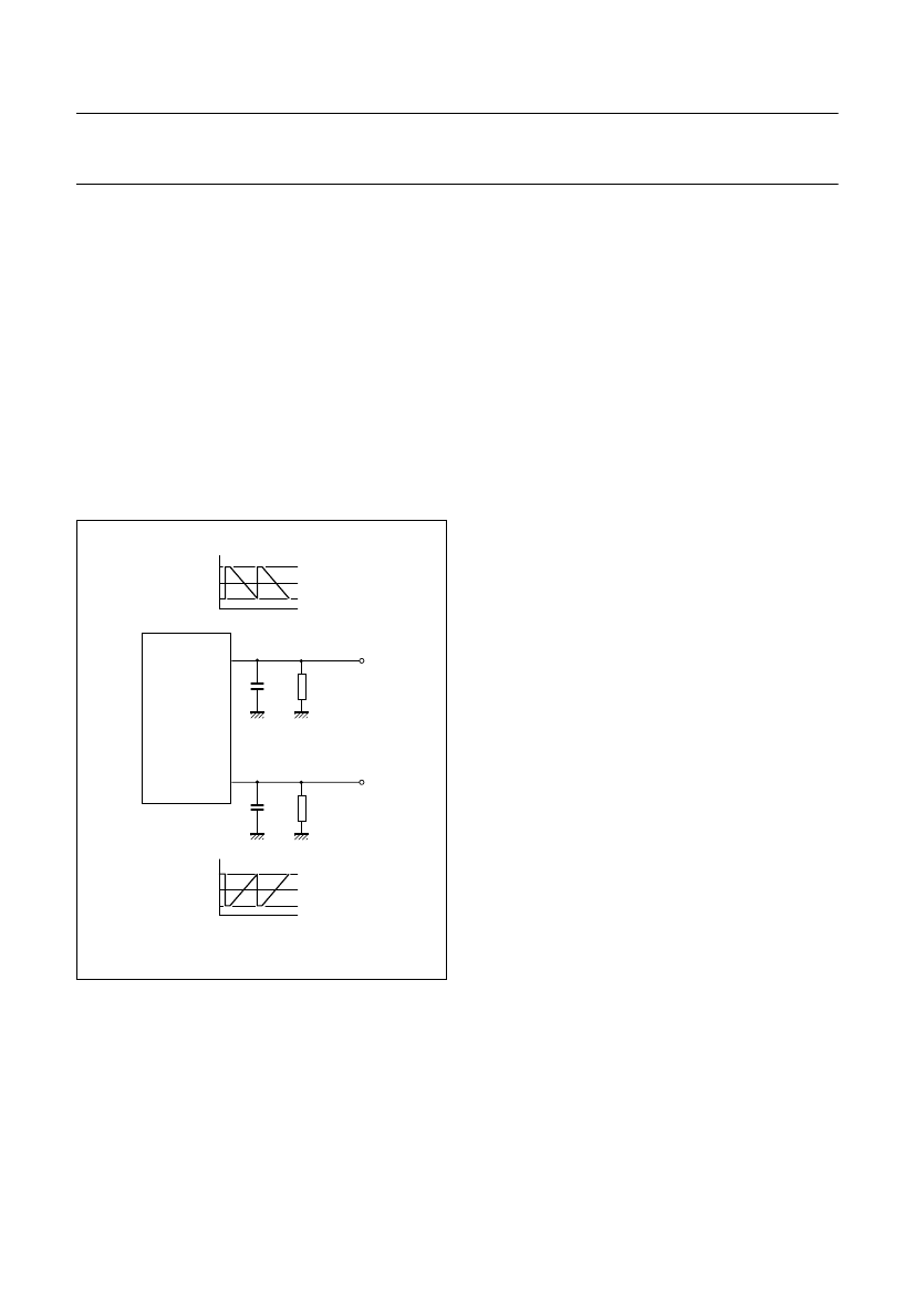
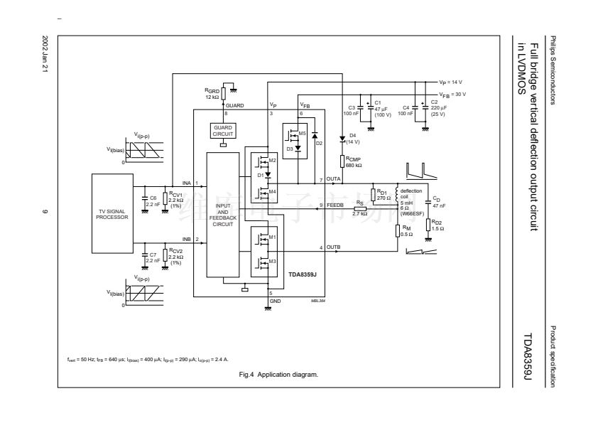
handbook, halfpage
Ii1(p-p)
II(bias)
0
INA
C6
2.2 nF
TV SIGNAL
PROCESSOR
RCV1
2.2 k鈩?/div>
1
The required power supply voltage V
P
for the first part of
the scan is given by:
V
P
(
1
)
=
I
coil
(
peak
)
脳 (
R
coil
+
R
M
)
鈥?/div>
L
coil
脳
2I
coil
(
peak
)
脳
f
vert
(
max
)
+
V
loss
(
1
)
INB
C7
2.2 nF
Ii2(p-p)
II(bias)
0
RCV2
2.2 k鈩?/div>
2
The required power supply voltage V
P
for the second part
of the scan is given by:
V
P
(
2
)
=
I
coil
(
peak
)
脳 (
R
coil
+
R
M
)
+
L
coil
脳
2I
coil
(
peak
)
脳
f
vert
(
max
)
+
V
loss
(
2
)
The minimum required supply voltage V
P
shall be the
highest of the two values V
P(1)
and V
P(2)
. Spread in supply
voltage and component values also has to be taken into
account.
MBL366
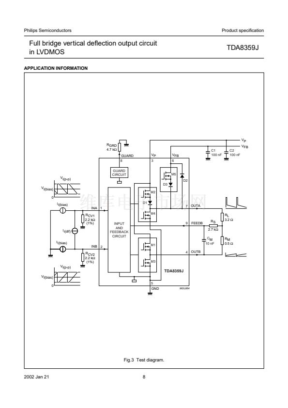
Fig.5 Input Circuit
E
XAMPLE
Measured or given values: I
I(bias)
= 400
碌A;
I
i1(p-p)
= I
i2(p-p)
=
290
碌A.
The differential input voltage will be:
V
i
(
dif
) (
p
鈥?/div>
p
)
=
290碌A
脳
2.2k鈩?/div>
鈥?/div>
(
鈥?/div>
290碌A
脳
2.2k鈩?/div>
)
=
1.27V
2002 Jan 21
10
TDA8359J相关型号PDF文件下载
-
型号
版本
描述
厂商
下载
-
英文版
Octuple 6-bit DACs with I2C-bus
PHILIPS
-
英文版
Octuple 6-bit DACs with I2C-bus
PHILIPS [N...
-
英文版
Smart card interface
PHILIPS
-
英文版
Smart card interface
PHILIPS [N...
-
英文版
Smart card interface
PHILIPS
-
英文版
Smart card interface
PHILIPS [N...
-
英文版
IC card interface
PHILIPS
-
英文版
IC card interface
PHILIPS [N...
-
英文版
IC card interface
PHILIPS
-
英文版
IC card interface
PHILIPS [N...
-
英文版
Low-power smart card coupler
PHILIPS
-
英文版
Low-power smart card coupler
PHILIPS [N...
-
英文版
Multiprotocol IC Card coupler
Philips
-
英文版
Dual multiprotocol smart card
Philips
-
英文版
Low power mixers/oscillators for satellite tuners
PHILIPS
-
英文版
Low power mixers/oscillators for satellite tuners
PHILIPS [N...
-
英文版
IF amplifier for satellite TV receivers
PHILIPS
-
英文版
IF amplifier for satellite TV receivers
PHILIPS [N...
-
英文版
Dual smart card interface
PHILIPS
-
英文版
Dual smart card interface
PHILIPS [N...


 1
1
 2
2
 3
3
 4
4
 5
5
 6
6
 7
7
 8
8
 9
9
 10
10
 11
11
 12
12
 13
13
 14
14
 15
15
 16
16
 17
17
 18
18
 19
19
 20
20
