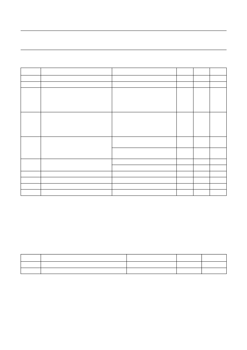
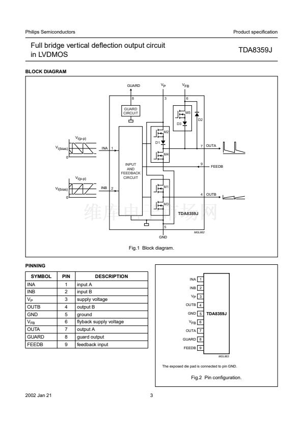
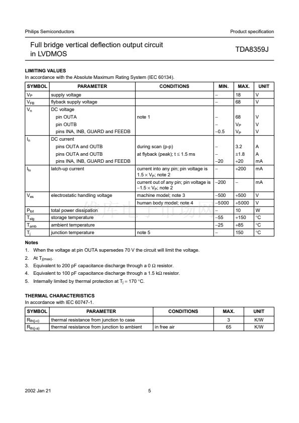
MIN.
MAX.
鈭?/div>
+500
+5000
10
+150
+85
150
UNIT
V
V
V
V
V
A
A
mA
mA
mA
V
V
W
掳C
掳C
掳C
current out of any pin; pin voltage is
鈭?00
鈭?.5 脳
V
P
; note 2
V
es
P
tot
T
stg
T
amb
T
j
Notes
1. When the voltage at pin OUTA supersedes 70 V the circuit will limit the voltage.
2. At T
j(max)
.
3. Equivalent to 200 pF capacitance discharge through a 0
鈩?/div>
resistor.
4. Equivalent to 100 pF capacitance discharge through a 1.5 k鈩?resistor.
5. Internally limited by thermal protection at T
j
=
170
掳C.
THERMAL CHARACTERISTICS
In accordance with IEC 60747-1.
SYMBOL
R
th(j-c)
R
th(j-a)
PARAMETER
thermal resistance from junction to case
thermal resistance from junction to ambient
in free air
CONDITIONS
MAX.
3
65
electrostatic handling voltage
total power dissipation
storage temperature
ambient temperature
junction temperature
note 5
machine model; note 3
human body model; note 4
鈭?00
鈭?000
鈭?/div>
鈭?5
鈭?5
鈭?/div>
UNIT
K/W
K/W
2002 Jan 21
5


 1
1
 2
2
 3
3
 4
4
 5
5
 6
6
 7
7
 8
8
 9
9
 10
10
 11
11
 12
12
 13
13
 14
14
 15
15
 16
16
 17
17
 18
18
 19
19
 20
20
