Philips Semiconductors
Product speci铿乧ation
Full bridge vertical de铿俥ction output circuit
in LVDMOS
FUNCTIONAL DESCRIPTION
Vertical output stage
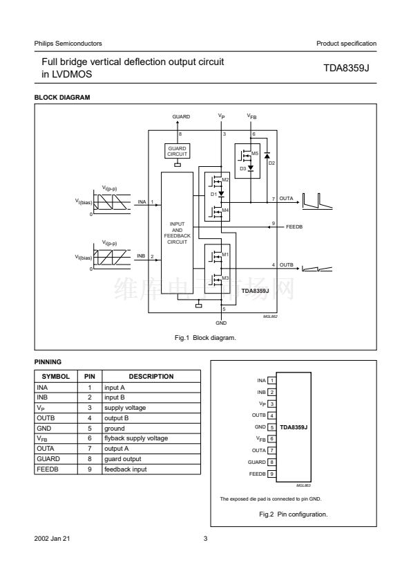
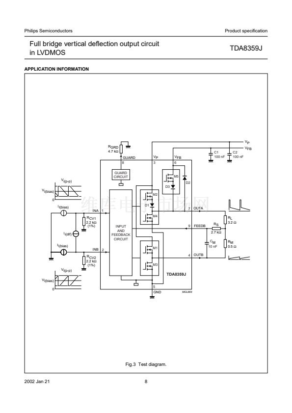
The vertical driver circuit has a bridge configuration. The
deflection coil is connected between the complimentary
driven output amplifiers. The differential input circuit is
voltage driven. The input circuit is specially designed for
direct connection to driver circuits delivering a differential
signal but it is also suitable for single-ended applications.
For processors with output currents, the currents are
converted to voltages by the conversion resistors
R
CV1
and R
CV2
(see Fig.5) connected to pins INA
and INB. The differential input voltage is compared with
the voltage across the measuring resistor R
M
, providing
feedback information. The voltage across R
M
is
proportional with the output current. The relationship
between the differential input voltage and the output
current is defined by:
V
i(dif)(p-p)
= I
o(p-p)
脳
R
M
V
i(dif)(p-p)
= V
INA
鈭?/div>
V
INB
The output current should not exceed 3.2 A (p-p) and is
determined by the value of R
M
and R
CV
. The allowable
input voltage range is 100 mV to 1.6 V for each input. The
formula given does not include internal bondwire
resistances. Depending on the values of R
M
and the
internal bondwire resistance (typical value of 50 m鈩? the
actual value of the current in the deflection coil will be
approximately 5% lower than calculated.
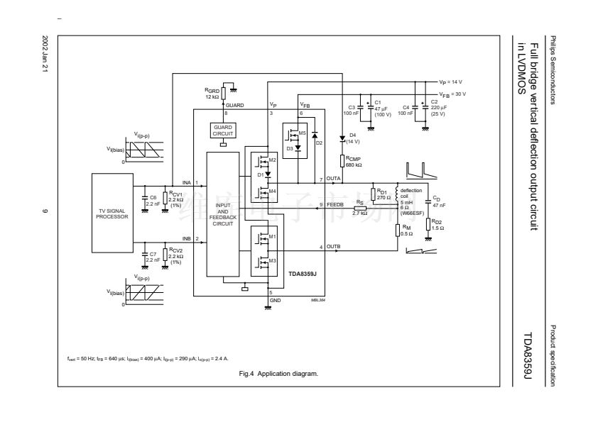
Flyback supply
The flyback voltage is determined by the flyback supply
voltage V
FB
. The principle of two supply voltages (class G)
allows to use an optimum supply voltage V
P
for scan and
an optimum flyback supply voltage V
FB
for flyback, thus
very high efficiency is achieved. The available flyback
output voltage across the coil is almost equal to V
FB
, due
to the absence of a coupling capacitor which is not
required in a bridge configuration. The very short rise and
fall times of the flyback switch are determined mainly by
the slew rate value of more than 300 V/碌s.
Protection
The output circuit contains protection circuits for:
鈥?/div>
Too high die temperature
鈥?/div>
Overvoltage of output A.
Guard circuit
TDA8359J
A guard circuit with output pin GUARD is provided.
The guard circuit generates a HIGH-level during the
flyback period. The guard circuit is also activated for one
of the following conditions:
鈥?/div>
During thermal protection (T
j
=
170
掳C)
鈥?/div>
During an open-loop condition.
The guard signal can be used for blanking the picture tube
and signalling fault conditions. The vertical
synchronization pulses of the guard signal can be used by
an On Screen Display (OSD) microcontroller.
Damping resistor compensation
HF loop stability is achieved by connecting a damping
resistor R
D1
across the deflection coil. The current values
in R
D1
during scan and flyback are significantly different.
Both the resistor current and the deflection coil current flow
into measuring resistor R
M
, resulting in a too low deflection
coil current at the start of the scan.
The difference in the damping resistor current values
during scan and flyback have to be externally
compensated in order to achieve a short settling time. For
that purpose a compensation resistor R
CMP
in series with
a zener diode is connected between pins OUTA and INA
(see Fig.4). The zener diode voltage value should be
equal to V
P
. The value of R
CMP
is calculated by:
(
V
FB
鈥?/div>
V
loss
(
FB
)
鈥?/div>
V
Z
) 脳
R
D1
脳
R
CV1
R
CMP
=
-----------------------------------------------------------------------------------------------------------
-
(
V
FB
鈥?/div>
V
loss
(
FB
)
鈥?/div>
I
coil
(
peak
)
脳
R
coil
) 脳
R
M
where:
鈥?/div>
V
loss(FB)
is the voltage loss between pins V
FB
and OUTA
at flyback
鈥?/div>
R
coil
is the deflection coil resistance
鈥?/div>
V
Z
is the voltage of zener diode D4.
2002 Jan 21
4
TDA8359J相关型号PDF文件下载
-
型号
版本
描述
厂商
下载
-
英文版
Octuple 6-bit DACs with I2C-bus
PHILIPS
-
英文版
Octuple 6-bit DACs with I2C-bus
PHILIPS [N...
-
英文版
Smart card interface
PHILIPS
-
英文版
Smart card interface
PHILIPS [N...
-
英文版
Smart card interface
PHILIPS
-
英文版
Smart card interface
PHILIPS [N...
-
英文版
IC card interface
PHILIPS
-
英文版
IC card interface
PHILIPS [N...
-
英文版
IC card interface
PHILIPS
-
英文版
IC card interface
PHILIPS [N...
-
英文版
Low-power smart card coupler
PHILIPS
-
英文版
Low-power smart card coupler
PHILIPS [N...
-
英文版
Multiprotocol IC Card coupler
Philips
-
英文版
Dual multiprotocol smart card
Philips
-
英文版
Low power mixers/oscillators for satellite tuners
PHILIPS
-
英文版
Low power mixers/oscillators for satellite tuners
PHILIPS [N...
-
英文版
IF amplifier for satellite TV receivers
PHILIPS
-
英文版
IF amplifier for satellite TV receivers
PHILIPS [N...
-
英文版
Dual smart card interface
PHILIPS
-
英文版
Dual smart card interface
PHILIPS [N...


 1
1
 2
2
 3
3
 4
4
 5
5
 6
6
 7
7
 8
8
 9
9
 10
10
 11
11
 12
12
 13
13
 14
14
 15
15
 16
16
 17
17
 18
18
 19
19
 20
20
