Philips Semiconductors
Product speci铿乧ation
Full bridge vertical de铿俥ction output circuit
in LVDMOS
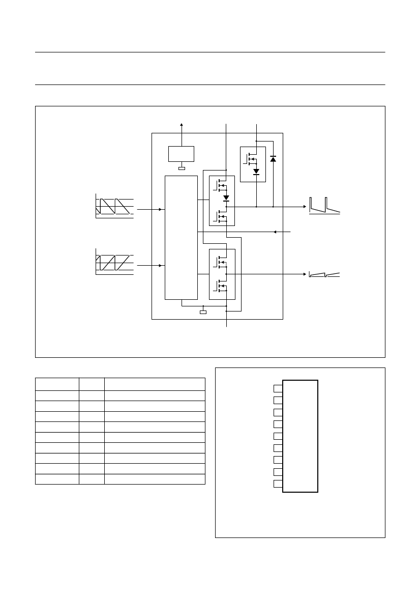
BLOCK DIAGRAM
handbook, full pagewidth
TDA8359J
GUARD
VP
VFB
8
GUARD
CIRCUIT
3
6
M5
D2
D3
M2
Vi(p-p)
D1
VI(bias)
0
INPUT
AND
FEEDBACK
CIRCUIT
INB
2
M1
4
M3
OUTB
INA
1
M4
9
FEEDB
7
OUTA
Vi(p-p)
VI(bias)
0
TDA8359J
5
MGL862
GND
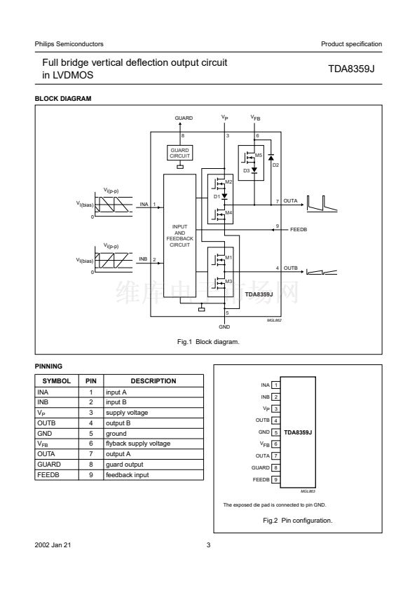
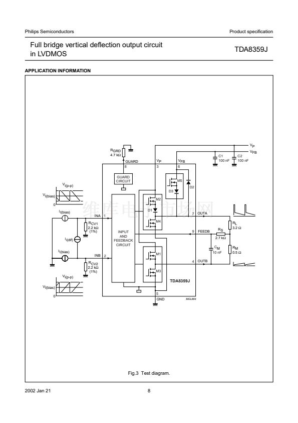
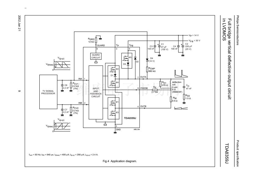
Fig.1 Block diagram.
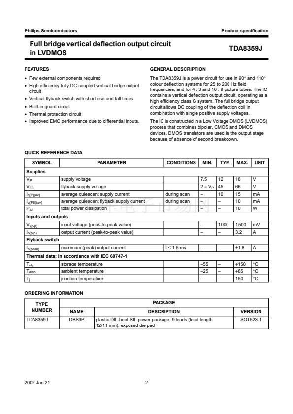
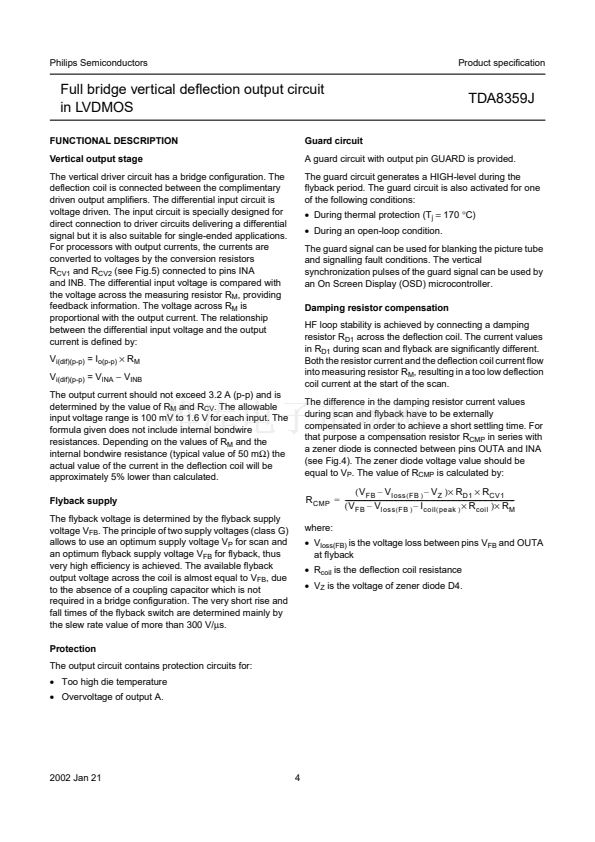
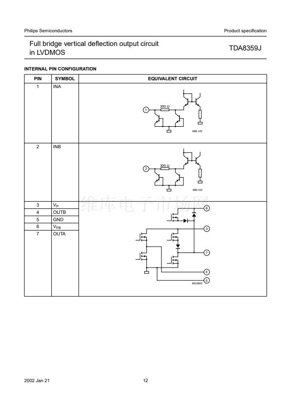
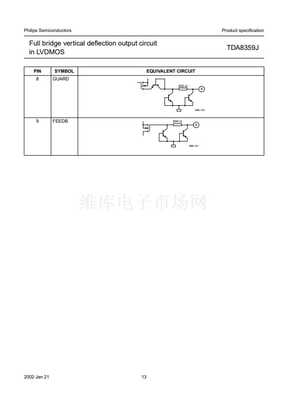
PINNING
SYMBOL
INA
INB
V
P
OUTB
GND
V
FB
OUTA
GUARD
FEEDB
PIN
1
2
3
4
5
6
7
8
9
input A
input B
supply voltage
output B
ground
铿倅back supply voltage
output A
guard output
feedback input
VP
OUTB
GND
VFB
OUTA
GUARD
FEEDB
3
4
5
6
7
8
9
MGL863
DESCRIPTION
handbook, halfpage
INA
INB
1
2
TDA8359J
The exposed die pad is connected to pin GND.
Fig.2 Pin configuration.
2002 Jan 21
3


 1
1
 2
2
 3
3
 4
4
 5
5
 6
6
 7
7
 8
8
 9
9
 10
10
 11
11
 12
12
 13
13
 14
14
 15
15
 16
16
 17
17
 18
18
 19
19
 20
20
