鈥?/div>
卤100ps
Cycle鈥搕o鈥揅ycle Jitter
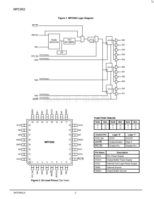
The MPC952 features three banks of individually configurable outputs.
The banks contain 5 outputs, 4 outputs and 2 outputs. The internal divide
circuitry allows for output frequency ratios of 1:1, 2:1, 3:1 and 3:2:1. The
output frequency relationship is controlled by the fsel frequency control
pins. The fsel pins as well as the other inputs are LVCMOS/LVTTL
compatible inputs.
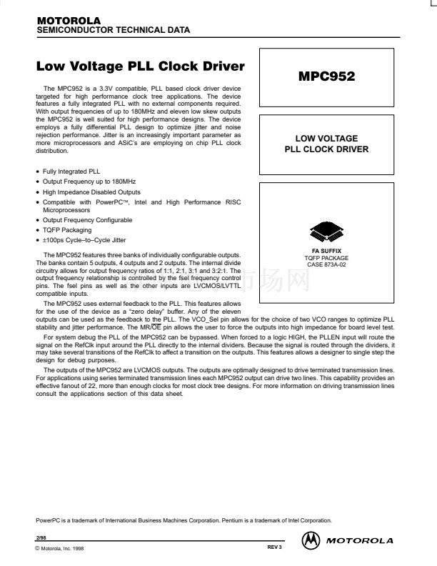
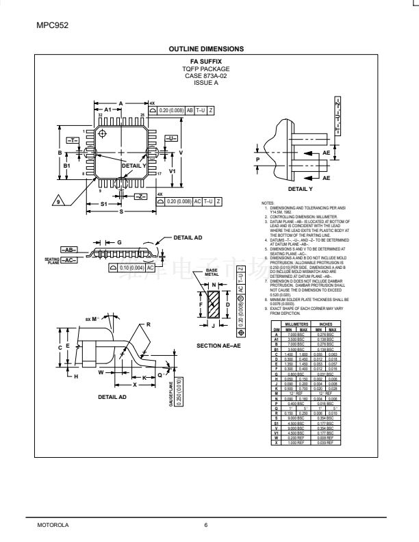
FA SUFFIX
TQFP PACKAGE
CASE 873A-02
The MPC952 uses external feedback to the PLL. This features allows
for the use of the device as a 鈥渮ero delay鈥?buffer. Any of the eleven
outputs can be used as the feedback to the PLL. The VCO_Sel pin allows for the choice of two VCO ranges to optimize PLL
stability and jitter performance. The MR/OE pin allows the user to force the outputs into high impedance for board level test.
For system debug the PLL of the MPC952 can be bypassed. When forced to a logic HIGH, the PLLEN input will route the
signal on the RefClk input around the PLL directly to the internal dividers. Because the signal is routed through the dividers, it
may take several transitions of the RefClk to affect a transition on the outputs. This features allows a designer to single step the
design for debug purposes.
The outputs of the MPC952 are LVCMOS outputs. The outputs are optimally designed to drive terminated transmission lines.
For applications using series terminated transmission lines each MPC952 output can drive two lines. This capability provides an
effective fanout of 22, more than enough clocks for most clock tree designs. For more information on driving transmission lines
consult the applications section of this data sheet.
PowerPC is a trademark of International Business Machines Corporation. Pentium is a trademark of Intel Corporation.
2/98
漏
Motorola, Inc. 1998
1
REV 3


 1
1
 2
2
 3
3
 4
4
 5
5
 6
6
 7
7
