鈥?/div>
6 Low Skew Clock Outputs
1 Dedicated PLL Feedback Output
Individual Output Enable Control
Fully Integrated PLL
Output Frequency Up TO 120MHz
32鈥搇ead TQFP Packaging
3.3V VCC
卤100ps
Cycle鈥揅ycle Jitter
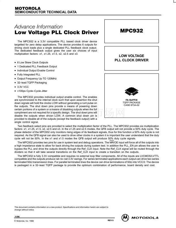
LOW VOLTAGE
PLL CLOCK DRIVER
The MPC932 provides individual output enable control. The enables
are synchronized to the internal clock such that upon assertion the shut
down signals will hold the clocks LOW without generating a runt pulse on
the outputs. The shut down pins provide a means of powering down
certain portions of a system or a means of disabling outputs when the full
compliment are not required for a specific design. The shut down pins will
disable the outputs when driven LOW. A common shut down pin is
provided to disable all of the outputs (except the feedback output) with a
single control signal.
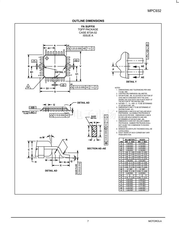
FA SUFFIX
TQFP PACKAGE
CASE 873A-02
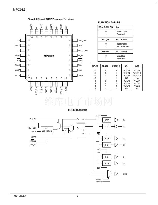
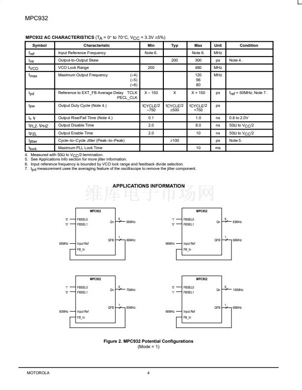
Two feedback select pins are provided to select the multiplication factor of the PLL. The MPC932 provides six multiplication
factors: x1, x1.25, x1.5, x2, x2.5 and x3. In the x1.25 and x2.5 modes, the QFB output will not provide a 50% duty cycle. The
phase detector of the MPC932 only monitors rising edges of its feedback signals, thus for this function a 50% duty cycle is not
required. As the QFB signal can also be used to drive other clocks in a system it is important the user understand that the duty
cycle will not be 50%. In the x1 and x1.5 modes the QFB output will produce 50% duty cycle signals.
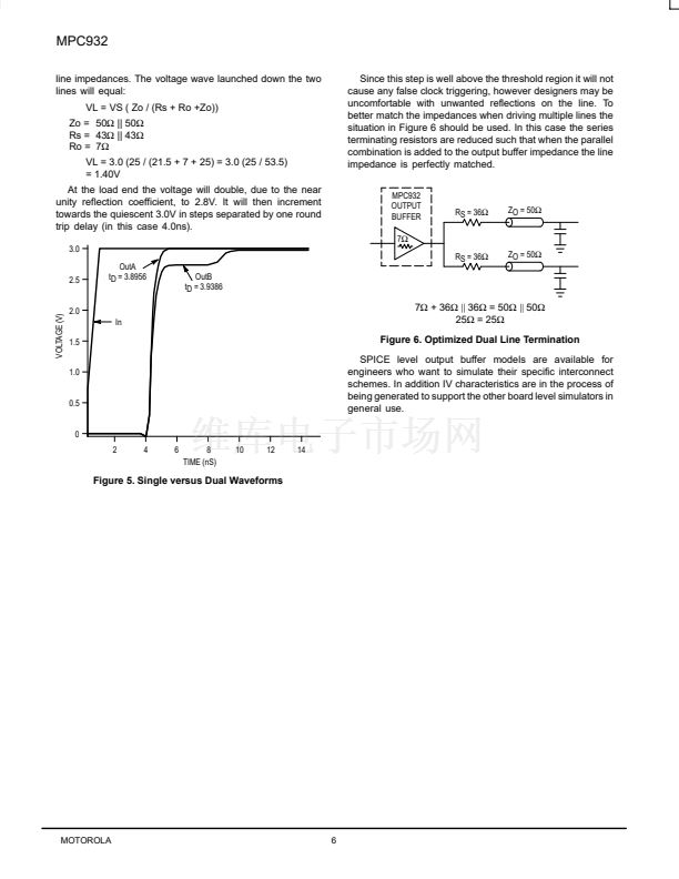
The MPC932 provides two pins for use in system test and debug operations. The MR/OE input will force all of the outputs into
a high impedance state to allow for back driving the outputs during system test. In addition the PLL_EN pin allows the user to
bypass the PLL and drive the outputs directly through the Ref_CLK input. Note the Ref_CLK signal will be routed through the
dividers so that it will take several transitions on the Ref_CLK input to create a transition on the outputs.
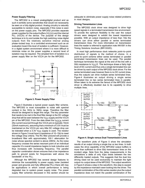
The MPC932 is fully 3.3V compatible and requires no external loop filter components. All of the inputs are LVCMOS/LVTTL
compatible and the outputs produce rail鈥搕o鈥搑ail 3.3V swings. For series terminated applications each output can drive two series
terminated 50鈩?transmission lines. For parallel terminated lines the device can drive terminations of 50鈩?into VCC/2. The device
is packaged in a 32鈥搇ead TQFP package to provide the optimum combination of performance, board density and cost.
This document contains information on a new product. Specifications and information herein are subject to
change without notice.
11/96
漏
Motorola, Inc. 1996
1
REV 0


 1
1
 2
2
 3
3
 4
4
 5
5
 6
6
 7
7
 8
8
