鈥?/div>
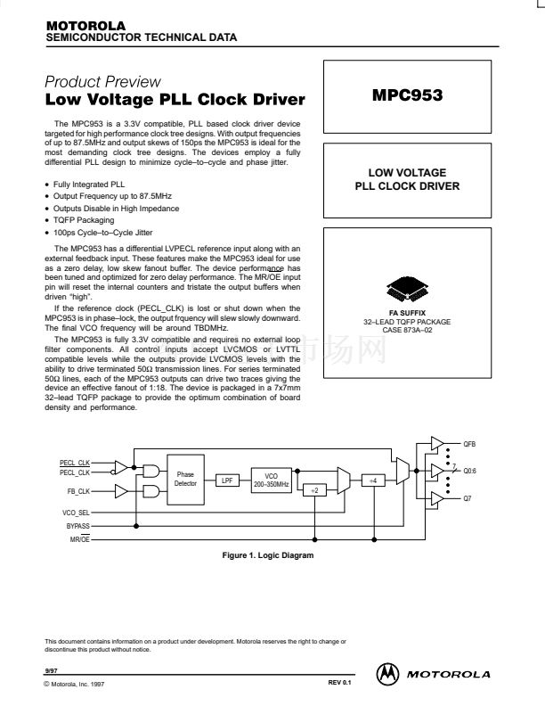
Fully Integrated PLL
Output Frequency up to 87.5MHz
Outputs Disable in High Impedance
TQFP Packaging
100ps Cycle鈥搕o鈥揅ycle Jitter
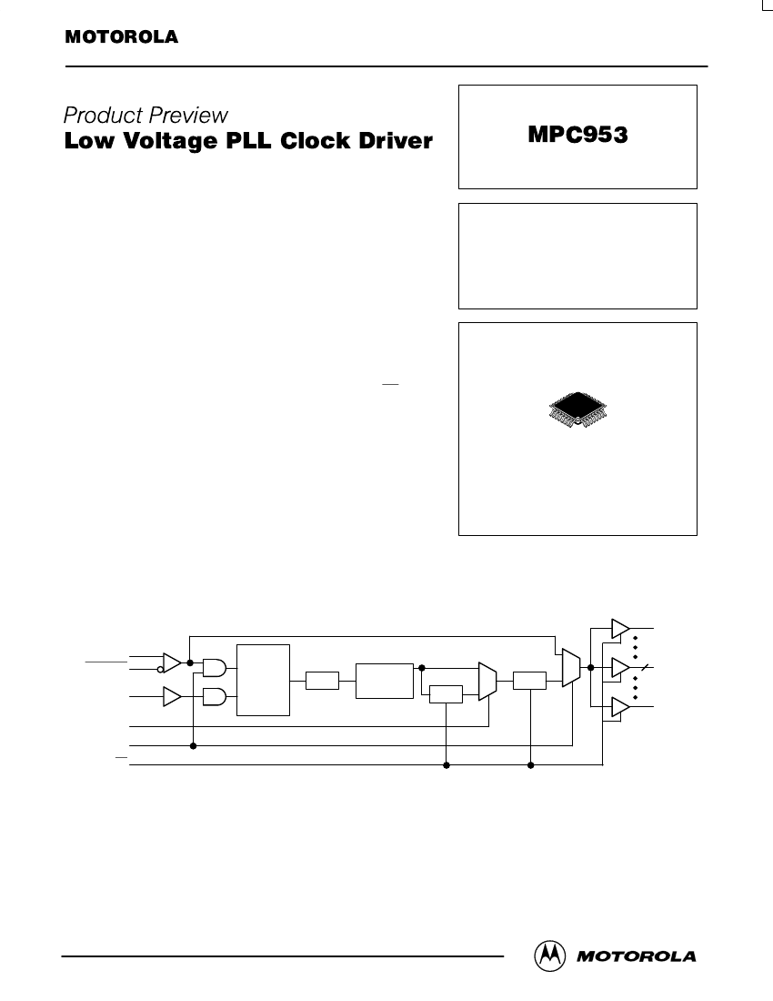
LOW VOLTAGE
PLL CLOCK DRIVER
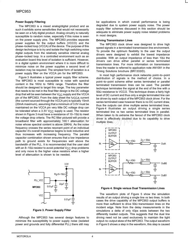
The MPC953 has a differential LVPECL reference input along with an
external feedback input. These features make the MPC953 ideal for use
as a zero delay, low skew fanout buffer. The device performance has
been tuned and optimized for zero delay performance. The MR/OE input
pin will reset the internal counters and tristate the output buffers when
driven 鈥渉igh鈥?
If the reference clock (PECL_CLK) is lost or shut down when the
MPC953 is in phase鈥搇ock, the output frquency will slew slowly downward.
The final VCO frequency will be around TBDMHz.
The MPC953 is fully 3.3V compatible and requires no external loop
filter components. All control inputs accept LVCMOS or LVTTL
compatible levels while the outputs provide LVCMOS levels with the
ability to drive terminated 50鈩?transmission lines. For series terminated
50鈩?lines, each of the MPC953 outputs can drive two traces giving the
device an effective fanout of 1:18. The device is packaged in a 7x7mm
32鈥搇ead TQFP package to provide the optimum combination of board
density and performance.
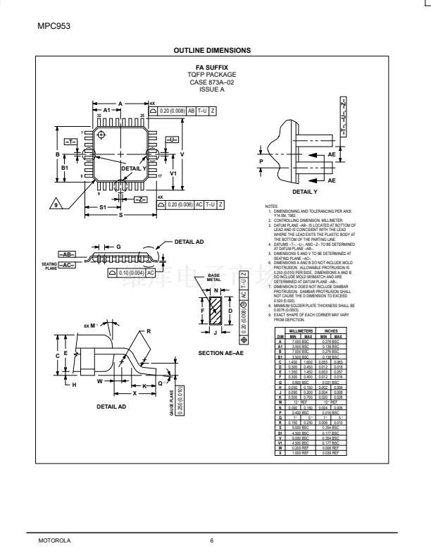
FA SUFFIX
32鈥揕EAD TQFP PACKAGE
CASE 873A鈥?2
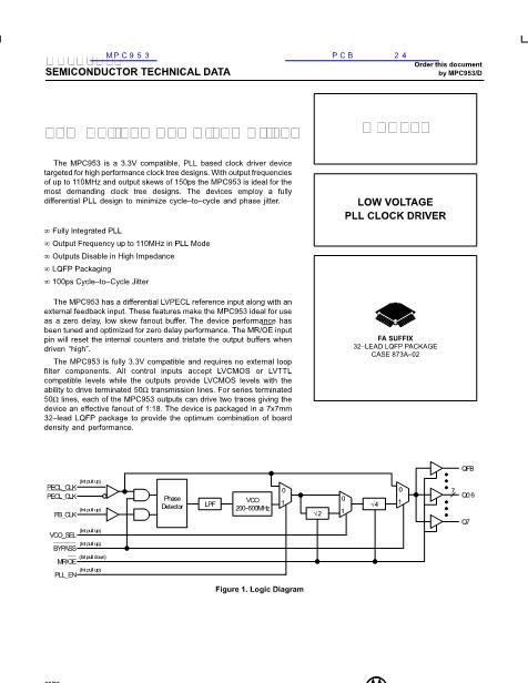
QFB
PECL_CLK
PECL_CLK
FB_CLK
VCO_SEL
BYPASS
MR/OE
7
Phase
Detector
LPF
VCO
200鈥?50MHz
梅4
梅2
Q7
Q0:6
Figure 1. Logic Diagram
This document contains information on a product under development. Motorola reserves the right to change or
discontinue this product without notice.
9/97
漏
Motorola, Inc. 1997
1
REV 0.1


 1
1
 2
2
 3
3
 4
4
 5
5
 6
6
 7
7
