鈥?/div>
Clock Distribution for Pentium鈩?Systems with PCI
Low Voltage PECL Clock Input
2 Selectable LVCMOS/LVTTL Clock Inputs
350ps Maximum Output to Output Skew
Drives up to 30 Independent Clock Lines
Maximum Output Frequency of 150MHz
High Impedance Output Enable
52鈥揕ead TQFP Packaging
3.3V VCC Supply
FA SUFFIX
52鈥揕EAD TQFP PACKAGE
CASE 848D鈥?3
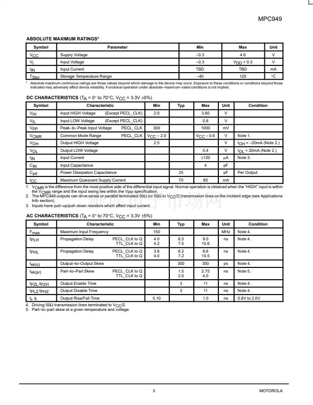
With an output impedance of approximately 7鈩? in both the HIGH and
the LOW logic states, the output buffers of the MPC949 are ideal for
driving series terminated transmission lines. More specifically each of the
15 MPC949 outputs can drive two series terminated transmission lines.
With this capability, the MPC949 has an effective fanout of 1:30 in
applications using point鈥搕o鈥損oint distribution schemes.
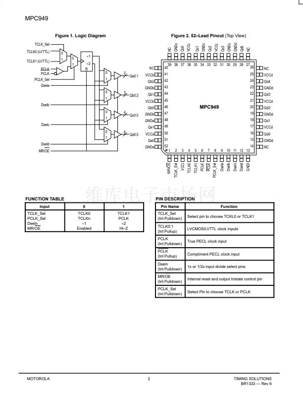
The MPC949 has the capability of generating 1X and 1/2X signals from a 1X source. The design is fully static, the signals are
generated and retimed inside the chip to ensure minimal skew between the 1X and 1/2X signals. The device features selectability
to allow the user to select the ratio of 1X outputs to 1/2X outputs.
Two independent LVCMOS/LVTTL compatible clock inputs are available. Designers can take advantage of this feature to
provide redundant clock sources or the addition of a test clock into the system design. With the TCLK_Sel input pulled HIGH the
TCLK1 input is selected. The PCLK_Sel input will select the PECL input clock when driven HIGH.
All of the control inputs are LVCMOS/LVTTL compatible. The Dsel pins choose between 1X and 1/2X outputs. A LOW on the
Dsel pins will select the 1X output. The MR/OE input will reset the internal flip flops and tristate the outputs when it is forced HIGH.
The MPC949 is fully 3.3V compatible. The 52 lead TQFP package was chosen to optimize performance, board space and cost
of the device. The 52鈥搇ead TQFP has a 10x10mm body size with a 0.65mm pin spacing.
Pentium is a trademark of Intel Corporation.
10/96
漏
Motorola, Inc. 1996
1
REV 1


 1
1
 2
2
 3
3
 4
4
 5
5
 6
6
