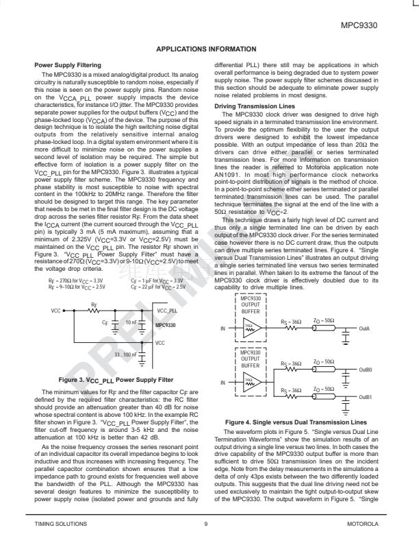
鈱┟?/div>
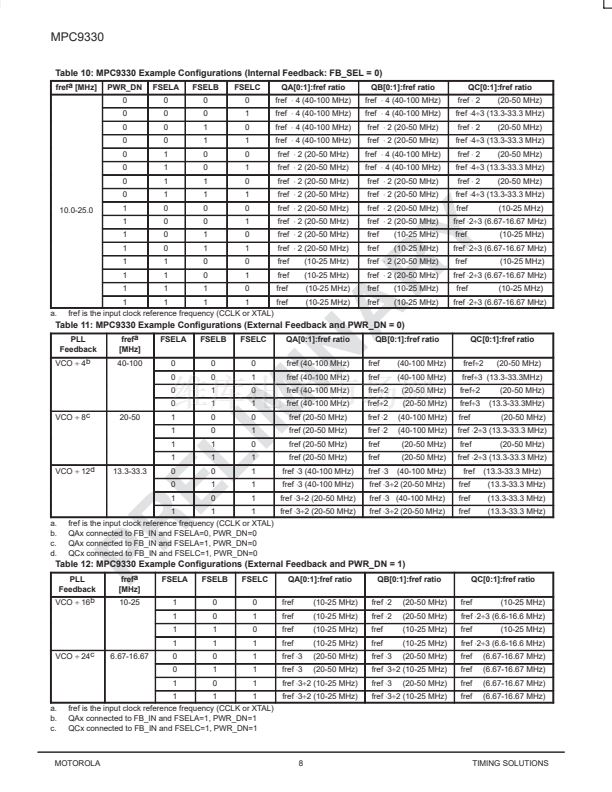
16 feedback)
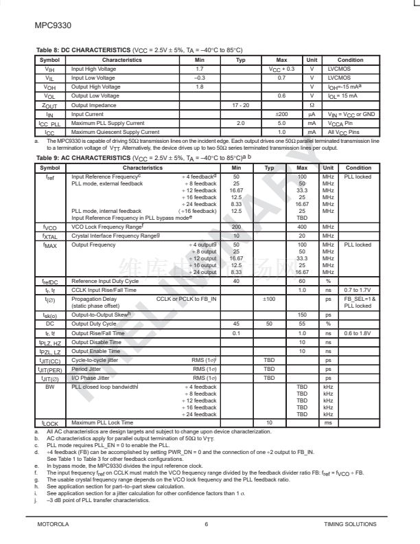
Input Reference Frequency in PLL bypass modee
VCO Lock Frequency Rangef
Crystal Interface Frequency Rangeg
Output Frequency
fVCO
fXTAL
fMAX
frefDC
tr, tf
t(鈭?
tsk(o)
DC
tr, tf
tPLZ, HZ
tPZL, LZ
tJIT(CC)
tJIT(PER)
tJIT(鈭?
BW
Reference Input Duty Cycle
CCLK Input Rise/Fall Time
Propagation Delay
(static phase offset)
Output-to-Output Skewh
Output Duty Cycle
Output Rise/Fall Time
Output Disable Time
Output Enable Time
Cycle-to-cycle jitter
Period Jitter
I/O Phase Jitter
PLL closed loop bandwidthj
PLL mode, external feedback
a.
b.
c.
d.
e.
f.
g.
h.
i.
j.
tLOCK
Maximum PLL Lock Time
10
ms
All AC characteristics are design targets and subject to change upon device characterization.
AC characteristics apply for parallel output termination of 50鈩?to VTT.
PLL mode requires PLL_EN = 0 to enable the PLL.
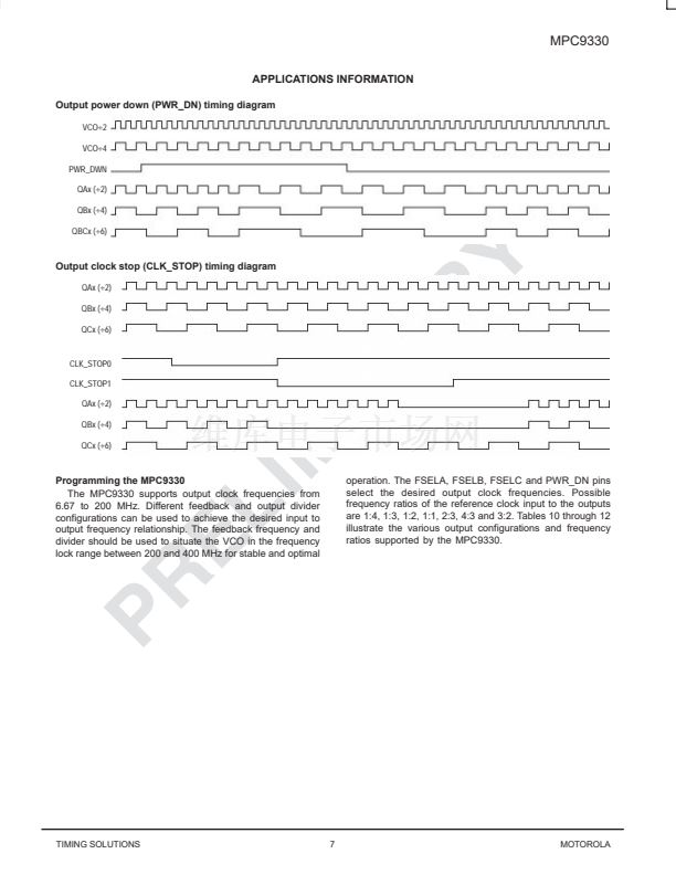
梅4
feedback (FB) can be accomplished by setting PWR_DN = 0 and the connection of one
梅2
output to FB_IN. See Table 1 to Table 3 for
other feedback configurations.
In bypass mode, the MPC9330 divides the input reference clock.
The input frequency fref on CCLK must match the VCO frequency range divided by the feedback divider ratio FB: fref = fVCO
梅
FB.
The usable crystal frequency range depends on the VCO lock frequency and the PLL feedback ratio.
See application section for part鈥搕o鈥損art skew calculation.
See application section for a jitter calculation for other confidence factors than 1
s
.
鈥? dB point of PLL transfer characteristics.
TIMING SOLUTIONS
5
MOTOROLA


 1
1
 2
2
 3
3
 4
4
 5
5
 6
6
 7
7
 8
8
 9
9
 10
10
 11
11
 12
12
 13
13
 14
14
 15
15
 16
16
