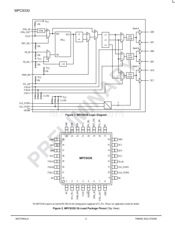
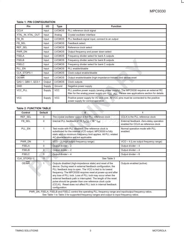
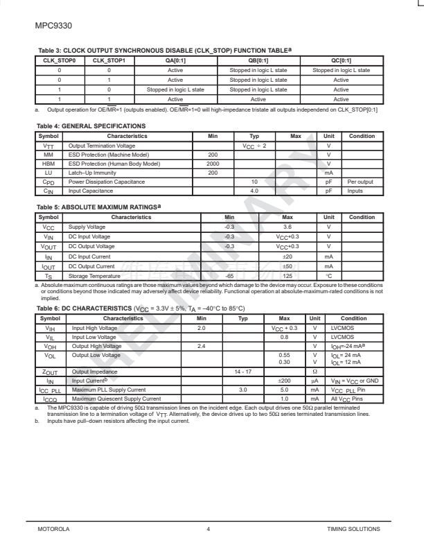
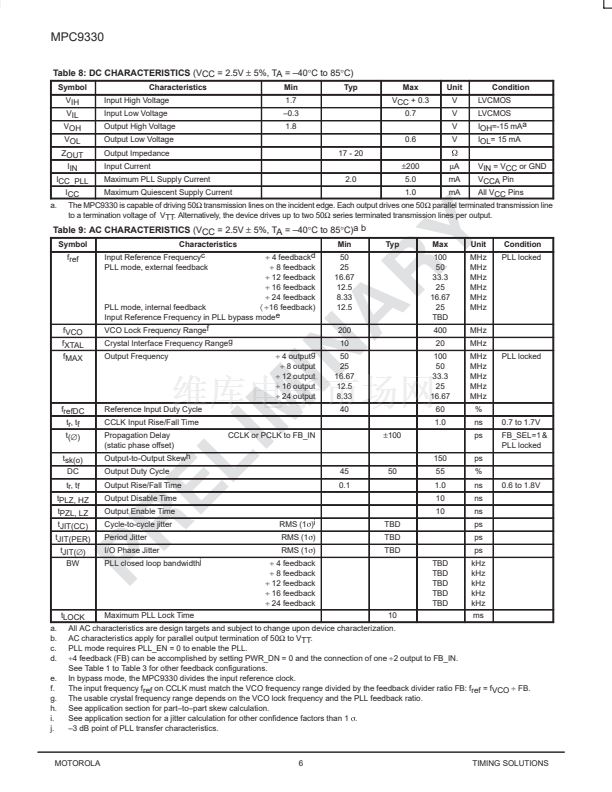
MPC9330
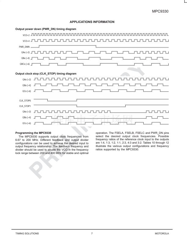
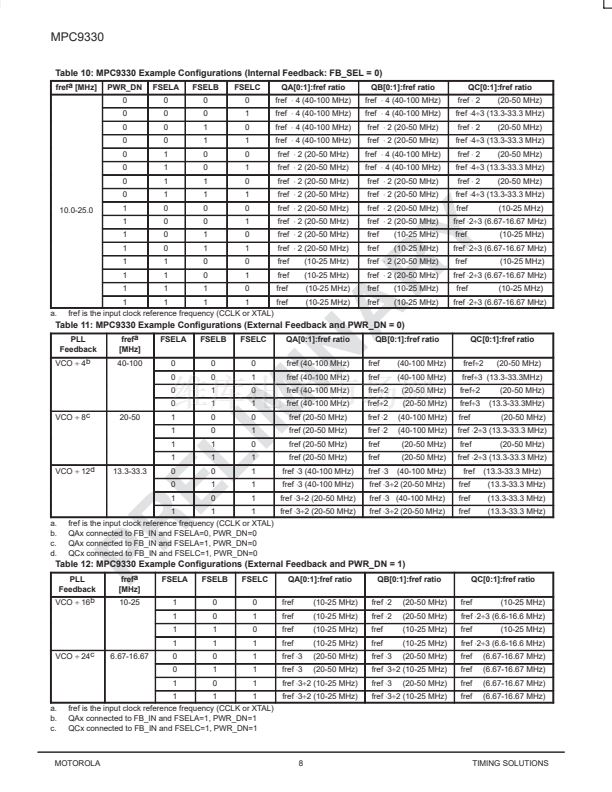
APPLICATIONS INFORMATION
Power Supply Filtering
The MPC9330 is a mixed analog/digital product. Its analog
circuitry is naturally susceptible to random noise, especially if
this noise is seen on the power supply pins. Random noise
on the VCCA_PLL power supply impacts the device
characteristics, for instance I/O jitter. The MPC9330 provides
separate power supplies for the output buffers (VCC) and the
phase-locked loop (VCCA) of the device. The purpose of this
design technique is to isolate the high switching noise digital
outputs from the relatively sensitive internal analog
phase-locked loop. In a digital system environment where it is
more difficult to minimize noise on the power supplies a
second level of isolation may be required. The simple but
effective form of isolation is a power supply filter on the
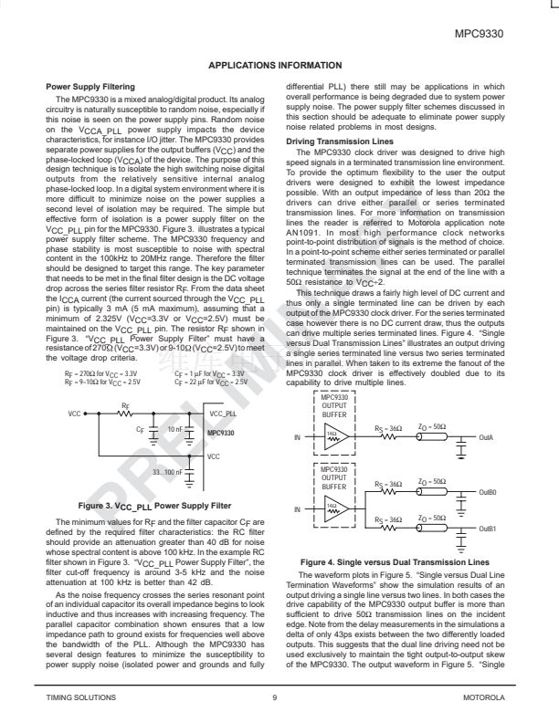
VCC_PLL pin for the MPC9330. Figure 3. illustrates a typical
power supply filter scheme. The MPC9330 frequency and
phase stability is most susceptible to noise with spectral
content in the 100kHz to 20MHz range. Therefore the filter
should be designed to target this range. The key parameter
that needs to be met in the final filter design is the DC voltage
drop across the series filter resistor RF. From the data sheet
the ICCA current (the current sourced through the VCC_PLL
pin) is typically 3 mA (5 mA maximum), assuming that a
minimum of 2.325V (VCC=3.3V or VCC=2.5V) must be
maintained on the VCC_PLL pin. The resistor RF shown in
Figure 3. 鈥淰CC_PLL Power Supply Filter鈥?must have a
resistance of 270 (VCC=3.3V) or 9-10 (VCC=2.5V) to meet
the voltage drop criteria.
differential PLL) there still may be applications in which
overall performance is being degraded due to system power
supply noise. The power supply filter schemes discussed in
this section should be adequate to eliminate power supply
noise related problems in most designs.
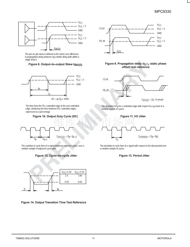
Driving Transmission Lines
The MPC9330 clock driver was designed to drive high
speed signals in a terminated transmission line environment.
To provide the optimum flexibility to the user the output
drivers were designed to exhibit the lowest impedance
possible. With an output impedance of less than 20鈩?the
drivers can drive either parallel or series terminated
transmission lines. For more information on transmission
lines the reader is referred to Motorola application note
AN1091. In most high performance clock networks
point-to-point distribution of signals is the method of choice.
In a point-to-point scheme either series terminated or parallel
terminated transmission lines can be used. The parallel
technique terminates the signal at the end of the line with a
50鈩?resistance to VCC
梅2.
This technique draws a fairly high level of DC current and
thus only a single terminated line can be driven by each
output of the MPC9330 clock driver. For the series terminated
case however there is no DC current draw, thus the outputs
can drive multiple series terminated lines. Figure 4. 鈥淪ingle
versus Dual Transmission Lines鈥?illustrates an output driving
a single series terminated line versus two series terminated
lines in parallel. When taken to its extreme the fanout of the
MPC9330 clock driver is effectively doubled due to its
capability to drive multiple lines.
MPC9330
OUTPUT
BUFFER
IN
14鈩?/div>
W
W
RF = 270鈩?for VCC = 3.3V
RF = 9鈥?0鈩?for VCC = 2.5V
RF
VCC
CF
CF = 1
碌F
for VCC = 3.3V
CF = 22
碌F
for VCC = 2.5V
VCC_PLL
10 nF
MPC9330
VCC
33...100 nF
RS = 36鈩?/div>
ZO = 50鈩?/div>
OutA
MPC9330
OUTPUT
BUFFER
IN
14鈩?/div>
RS = 36鈩?/div>
ZO = 50鈩?/div>
OutB0
Figure 3. VCC_PLL Power Supply Filter
The minimum values for RF and the filter capacitor CF are
defined by the required filter characteristics: the RC filter
should provide an attenuation greater than 40 dB for noise
whose spectral content is above 100 kHz. In the example RC
filter shown in Figure 3. 鈥淰CC_PLL Power Supply Filter鈥? the
filter cut-off frequency is around 3-5 kHz and the noise
attenuation at 100 kHz is better than 42 dB.
As the noise frequency crosses the series resonant point
of an individual capacitor its overall impedance begins to look
inductive and thus increases with increasing frequency. The
parallel capacitor combination shown ensures that a low
impedance path to ground exists for frequencies well above
the bandwidth of the PLL. Although the MPC9330 has
several design features to minimize the susceptibility to
power supply noise (isolated power and grounds and fully
RS = 36鈩?/div>
ZO = 50鈩?/div>
OutB1
Figure 4. Single versus Dual Transmission Lines
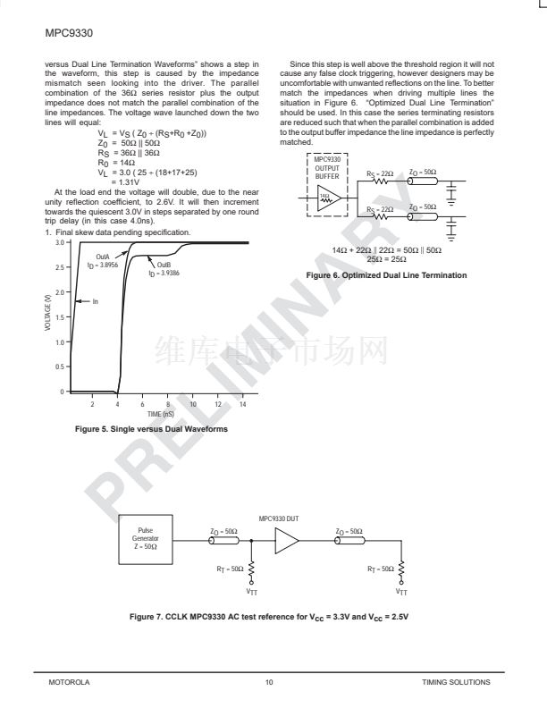
The waveform plots in Figure 5. 鈥淪ingle versus Dual Line
Termination Waveforms鈥?show the simulation results of an
output driving a single line versus two lines. In both cases the
drive capability of the MPC9330 output buffer is more than
sufficient to drive 50鈩?transmission lines on the incident
edge. Note from the delay measurements in the simulations a
delta of only 43ps exists between the two differently loaded
outputs. This suggests that the dual line driving need not be
used exclusively to maintain the tight output-to-output skew
of the MPC9330. The output waveform in Figure 5. 鈥淪ingle
TIMING SOLUTIONS
9
MOTOROLA
MPC9330相关型号PDF文件下载
-
型号
版本
描述
厂商
下载
-
英文版
Motorola, Inc [1:6 PCI CLOCK GENERATOR/ FANOUT BUFFER]
-
英文版
1:6 PCI CLOCK GENERATOR/ FANOUT BUFFER
-
英文版
1:6 PCI Clock Qenerator/Fanout Buffer
-
英文版
Motorola, Inc [LOW VOLTAGE CMOS 1:18 CLOCK DISTRIBUTION CHI...
-
英文版
Motorola, Inc [LOW-VOLTAGE 1:9 DIFFERENTIAL ECL/HSTL TO HST...
-
英文版
Low Voltage PLL Clock Drlver
-
英文版
Low Voltage PLL Clock Drlver
-
英文版
Motorola, Inc [LOW VOLTAGE PLL CLOCK DRIVER]
-
英文版
Motorola, Inc [LOW VOLTAGE 1:18 CLOCK DISTRIBUTION CHIP]
-
英文版
Low Voltage 1:27 Clock Dlstrlbutlon Chlp
-
英文版
Motorola, Inc [LOW VOLTAGE 1:10 CMOS CLOCK DRIVER]
-
英文版
Motorola, Inc [LOW VOLTAGE 1:9 CLOCK DISTRIBUTION CHIP]
-
英文版
Motorola, Inc [LOW VOLTAGE 1:12 CLOCK DISTRIBUTION CHIP]
-
英文版
Motorola, Inc [LOW VOLTAGE 1:15 PECL TO CMOS CLOCK DRIVER]
-
英文版
Low Voltage PLL Clock Drlver
-
英文版
Low Voltage PLL Clock Drlver
-
英文版
Low Voltage PLL Clock Drlver
-
英文版
Low Voltage PLL Clock Drlver
-
英文版
Low Voltage PLL Clock Drlver
-
英文版
Low Voltage PLL Clock Drlver


 1
1
 2
2
 3
3
 4
4
 5
5
 6
6
 7
7
 8
8
 9
9
 10
10
 11
11
 12
12
 13
13
 14
14
 15
15
 16
16
