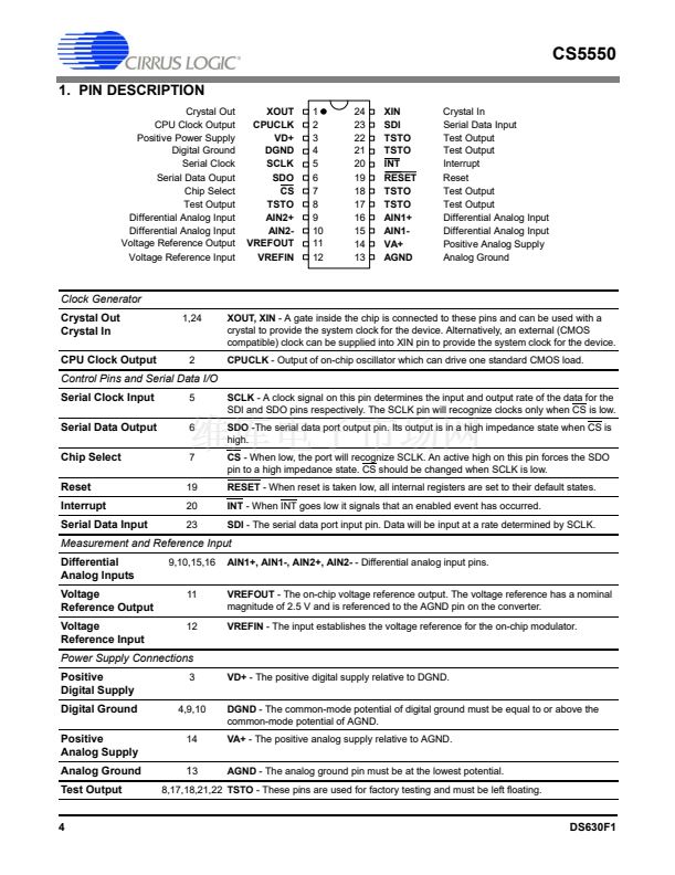
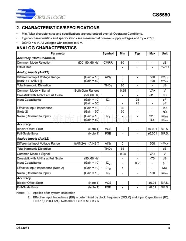
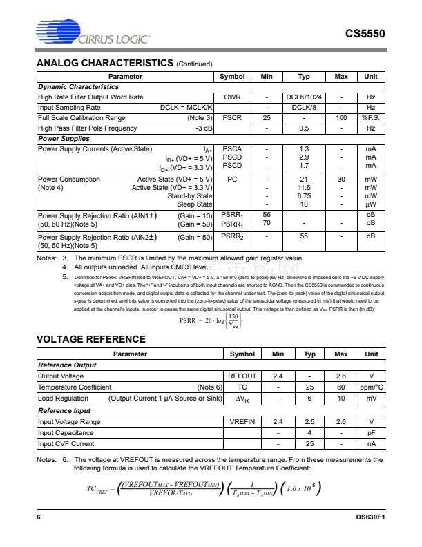
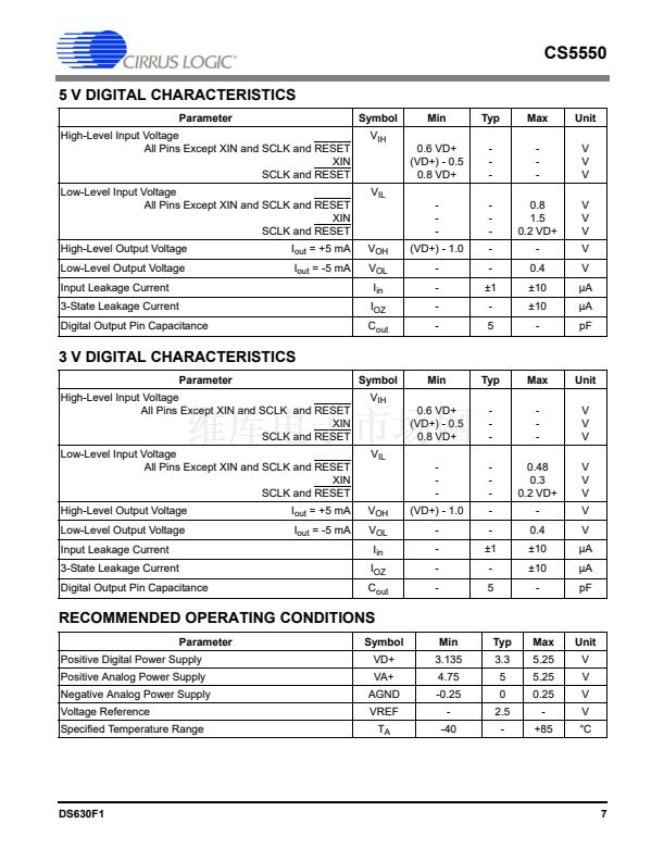
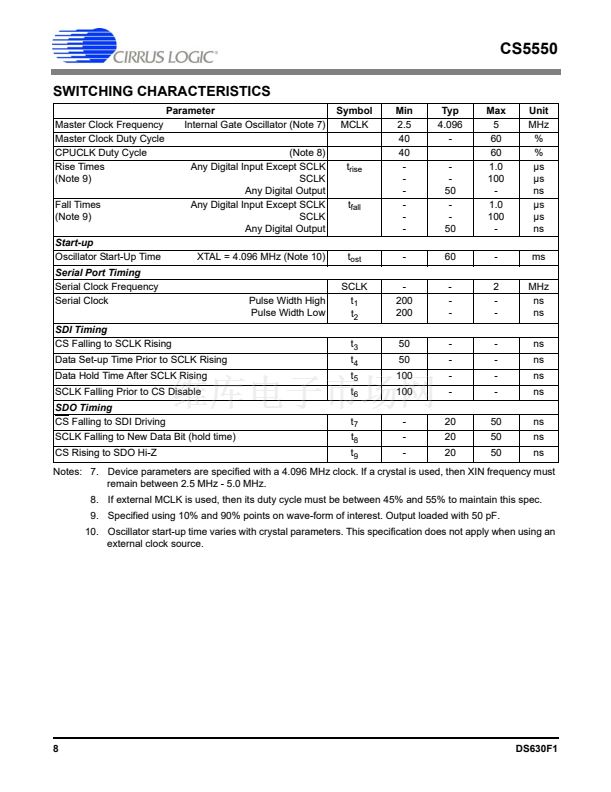
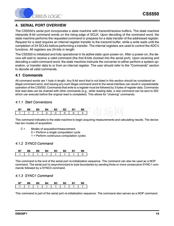
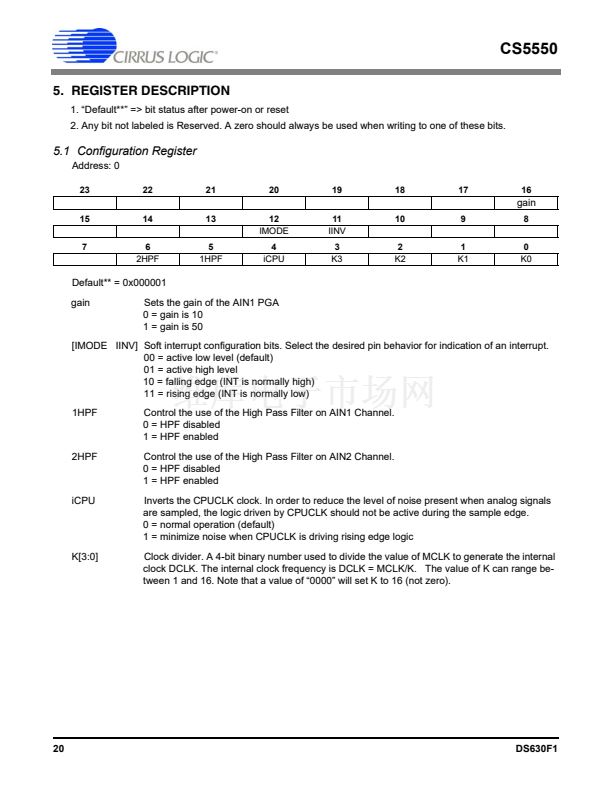
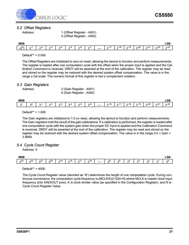
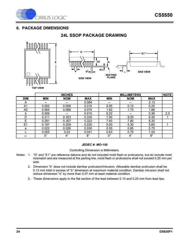
CS5550
3.4 Calibration
3.4.1 Overview of Calibration Process
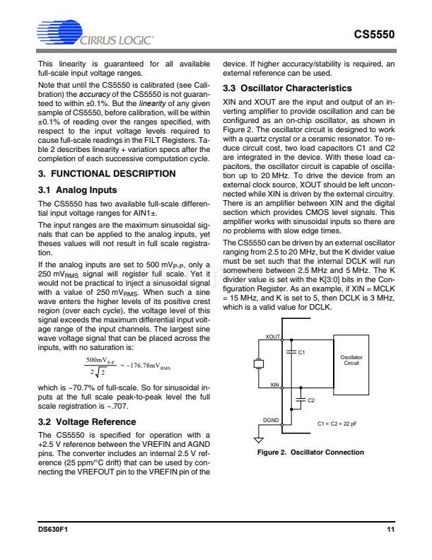
The CS5550 offers digital calibration for offset and
gain. Since both channels have separate offset
and gain registers associated with them, system
offset or system gain can be performed on either
channel without the calibration results from one
channel affecting the other.
maximum
instantaneous voltage level that needs
to be measured across the inputs (including the
maximum over-range level that must be accurately
measured).
For offset calibrations, the 鈥?鈥?and 鈥?鈥?pins of the
AIN
卤
channels should be connected to their
ground reference level. (See Figure 4.)
Calibrating both offset and gain at the same time
will cause undesirable calibration results.
External
C onnections
+
F ull +
Scale -
A IN +
XG AIN
-
CM
3.4.2 Calibration Sequence
1. Before Calibration the CS5550 must be operat-
ing in its
active
state, and ready to accept valid
commands. The 鈥楧RDY鈥?bit in the Status Register
should also be cleared.
2. Apply appropriate calibration signals to the in-
puts of the AIN1 and AIN2 channels (discussed
next in Sections 3.4.3 and 3.4.4.)
3. Send the 8-bit calibration command to the
CS5550 serial interface. Various bits within this
command specify the exact type of calibration. The
calibration command should not be sent to the de-
vice while performing A/D conversions.
4. After the CS5550 finishes the desired internal
calibration sequence, the DRDY bit is set in the
Status Register to indicate that the calibration se-
quence is complete. The results of the calibration
are now available in the appropriate gain/offset
registers.
+
-
+
-
AIN-
Figure 3. System Calibration of Gain.
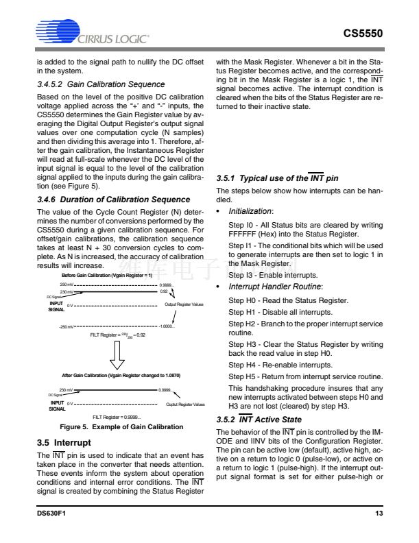
External
Connections
+
AIN+
0V +
-
-
CM +
-
AIN-
XGAIN
-
+
Figure 4. System Calibration of Offset.
3.4.3 Calibration Signal Input Level
For gain calibrations, there is an absolute limit on
the voltage levels that are selected for the gain cal-
ibration input signals. The maximum value that the
gain register can attain is 4. Therefore, for either
channel, if the voltage level of a gain calibration in-
put signal is low enough that it causes the CS5550
to attempt to set either gain register higher than 4,
the gain calibration result will be invalid and all
CS5550 results obtained while performing A/D
conversions will be invalid.
3.4.5 Description of Calibration Algo-
rithms
Note:
For proper calibration, the value of the
AIN1/AIN2 Gain Registers must be set to default (1.0)
before running the
gain
calibration(s), and the value in
the
Offset
Registers must be set to default (0) before
running
offset
calibrations. This can be accomplished
by a software or hardware reset of the device. The
values in the calibration registers
do
affect the results
of the calibration sequences.
3.4.4 Input Configurations for Calibrations
Figure 3 shows the basic setup for gain calibration.
When performing a gain calibration a
positive
DC
voltage level must be applied at the inputs of the
AIN1 and/or AIN2 channels. This voltage should
be set to the level that represents the
absolute
3.4.5.1 Offset Calibration Sequence
The Offset Registers hold the negative of the sim-
ple average of N samples taken while the offset
calibration was executed. The inputs should be
grounded during offset calibration. The offset value
12
DS630F1


 1
1
 2
2
 3
3
 4
4
 5
5
 6
6
 7
7
 8
8
 9
9
 10
10
 11
11
 12
12
 13
13
 14
14
 15
15
 16
16
 17
17
 18
18
 19
19
 20
20
 21
21
 22
22
 23
23
 24
24
