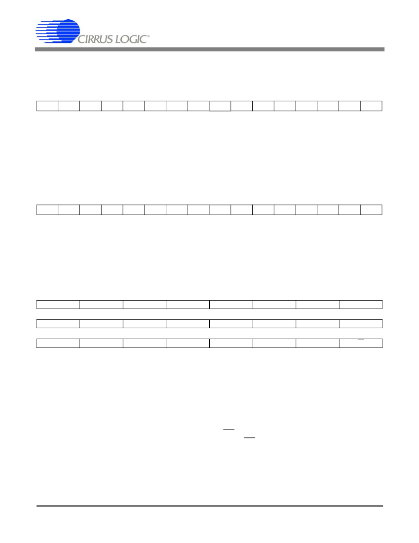
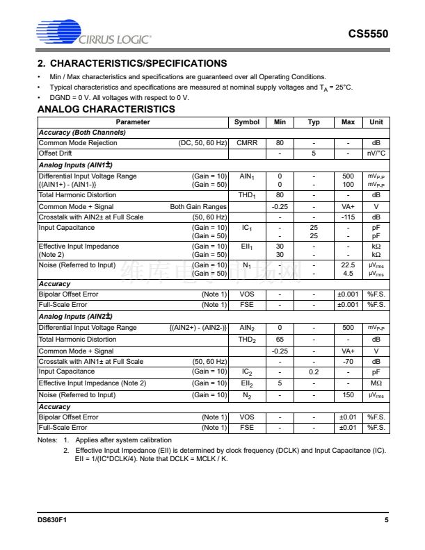
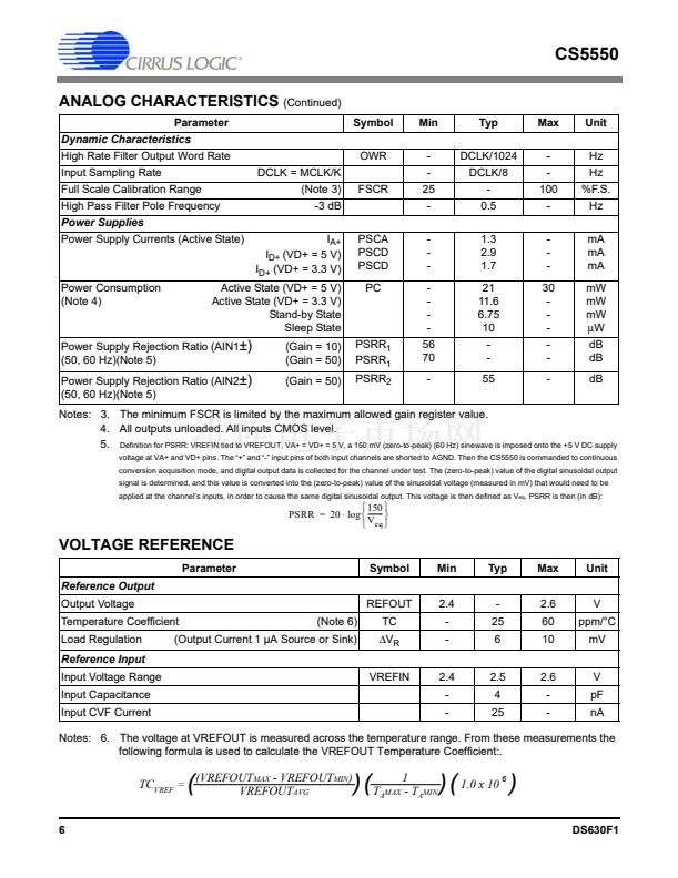
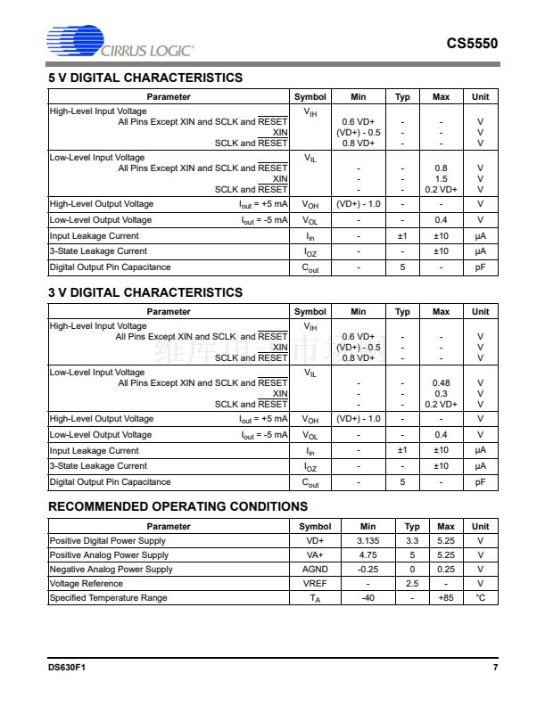
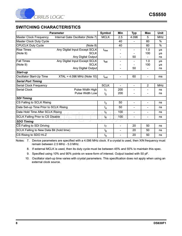
1.0. The value is represented in two's complement notation, with the binary
point place to the right of the MSB (MSB has a negative weighting). These values are 22 bits in length. The two
least significant bits, (located at the far right-side) have no meaning, and will always have a value of 鈥?鈥?
.....
. The results are in the range of
鈮?/div>
FILT
1
,FILT
2
<
1.0. The value is represented in (unsigned) binary notation, with the binary point place to
the left of the MSB. These results are updated after each computation cycle.
5.7 Status Register and Mask Register
Address:
Address:
23
DRDY
15
7
15
(Status
[Clear] Register)
26 (Mask Register)
22
14
FOR1
6
21
13
FOR2
5
20
CRDY
12
4
OD2
19
11
3
OD1
18
10
2
17
OR1
9
1
16
OR2
8
0
IC
Default** = 0x000000 (Status [Clear] Register
0x000000 (Mask Register)
The Status [Clear] Register indicates the condition of the chip. In normal operation writing a '1' to a bit will cause
the bit to go to the '0' state. Writing a '0' to a bit will maintain the status bit in its current state. With this feature
the user can simply write back to the Status [Clear] Register to clear the bits that have been seen, without con-
cern of clearing any newly set bits. Even if a status bit is masked to prevent the interrupt (at the time that the
status bit is asserted), the status bit will still be set in (both of) the Status Registers so the user can poll the status.
The Mask Register is used to control the activation of the INT pin. Placing a logic '1' in the Mask Register will
allow the corresponding bit in the Status Register to activate the INT pin when the status bit becomes active.
DRDY
Data Ready. When running in single or continuous conversion acquisition mode, this bit will in-
dicate the end of computation cycles. When running calibrations, this bit indicates that the cal-
ibration sequence has completed, and the results have been stored in the offset or gain
AIN Output Out of Range. Set when the
magnitude
of the calibrated output is too large or too
OR1, OR2
22
DS630F1


 1
1
 2
2
 3
3
 4
4
 5
5
 6
6
 7
7
 8
8
 9
9
 10
10
 11
11
 12
12
 13
13
 14
14
 15
15
 16
16
 17
17
 18
18
 19
19
 20
20
 21
21
 22
22
 23
23
 24
24
