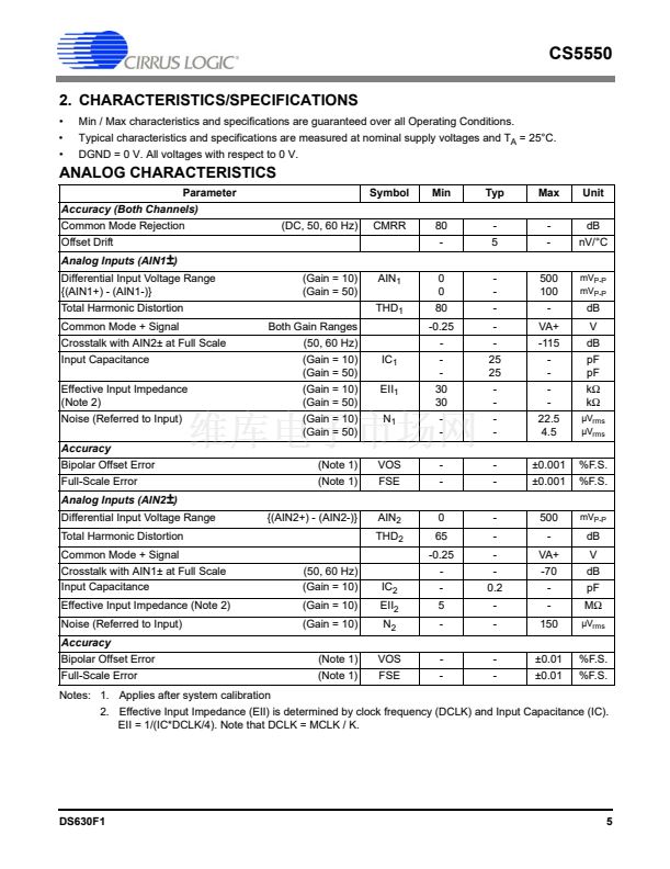
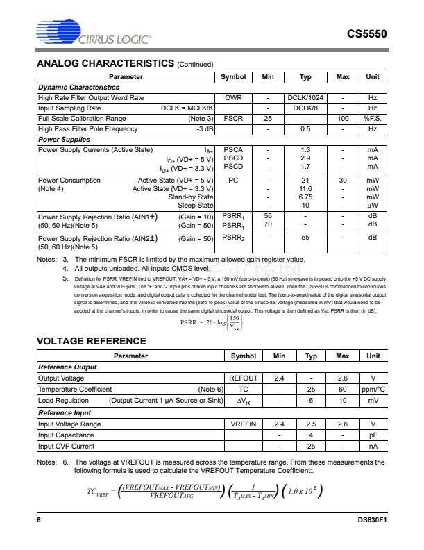
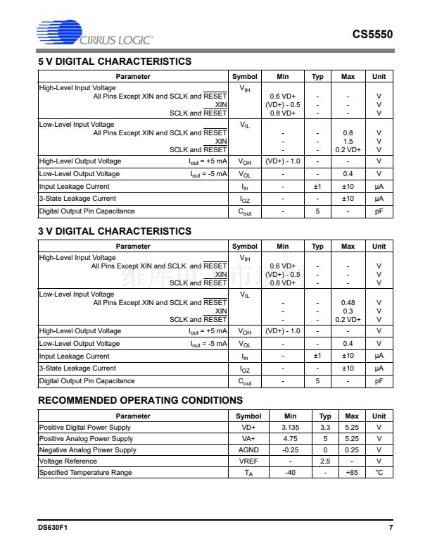
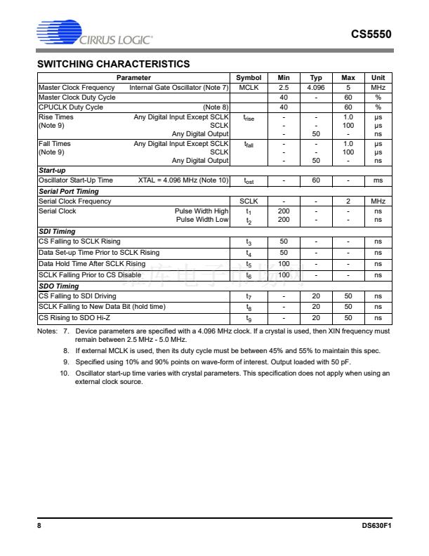
CS5550
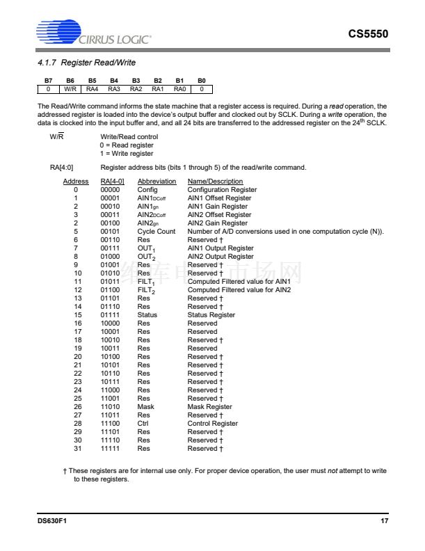
5. REGISTER DESCRIPTION
1. 鈥淒efault**鈥?=> bit status after power-on or reset
2. Any bit not labeled is Reserved. A zero should always be used when writing to one of these bits.
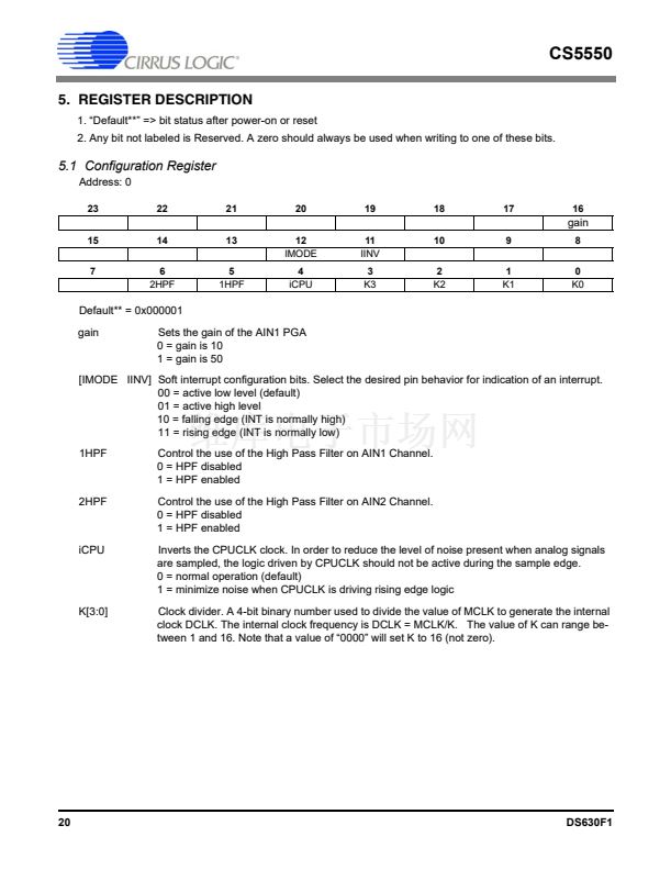
5.1 Configuration Register
Address: 0
23
15
7
22
14
6
2HPF
21
13
5
1HPF
20
12
IMODE
4
iCPU
19
11
IINV
3
K3
18
10
2
K2
17
9
1
K1
16
gain
8
0
K0
Default** = 0x000001
gain
Sets the gain of the AIN1 PGA
0 = gain is 10
1 = gain is 50
[IMODE IINV] Soft interrupt configuration bits. Select the desired pin behavior for indication of an interrupt.
00 = active low level (default)
01 = active high level
10 = falling edge (INT is normally high)
11 = rising edge (INT is normally low)
1HPF
Control the use of the High Pass Filter on AIN1 Channel.
0 = HPF disabled
1 = HPF enabled
Control the use of the High Pass Filter on AIN2 Channel.
0 = HPF disabled
1 = HPF enabled
Inverts the CPUCLK clock. In order to reduce the level of noise present when analog signals
are sampled, the logic driven by CPUCLK should not be active during the sample edge.
0 = normal operation (default)
1 = minimize noise when CPUCLK is driving rising edge logic
Clock divider. A 4-bit binary number used to divide the value of MCLK to generate the internal
clock DCLK. The internal clock frequency is DCLK = MCLK/K. The value of K can range be-
tween 1 and 16. Note that a value of 鈥?000鈥?will set K to 16 (not zero).
2HPF
iCPU
K[3:0]
20
DS630F1


 1
1
 2
2
 3
3
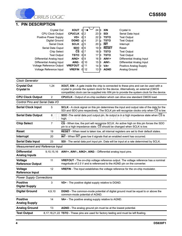 4
4
 5
5
 6
6
 7
7
 8
8
 9
9
 10
10
 11
11
 12
12
 13
13
 14
14
 15
15
 16
16
 17
17
 18
18
 19
19
 20
20
 21
21
 22
22
 23
23
 24
24
