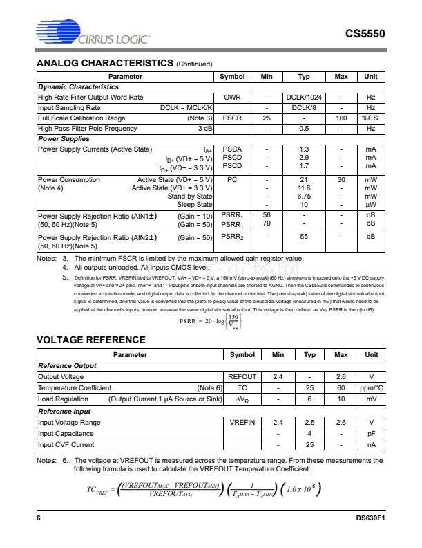
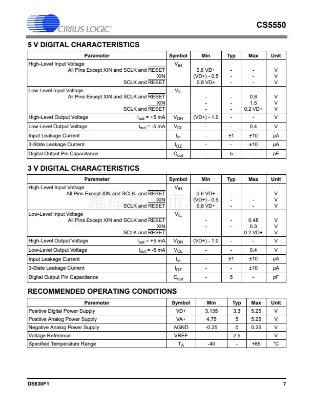
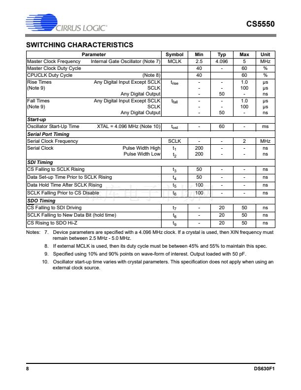
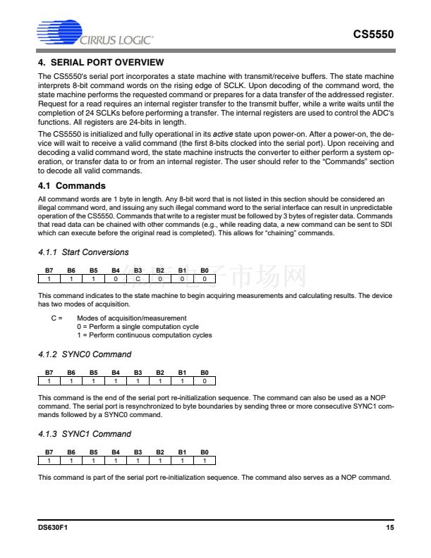
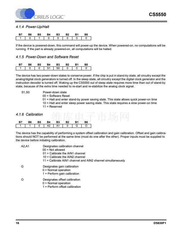
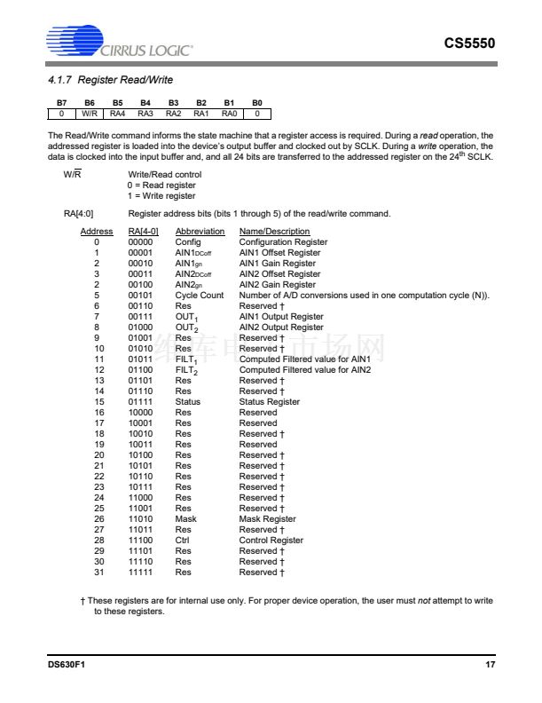
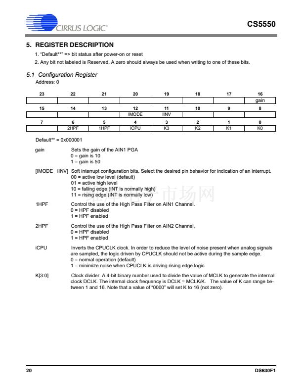
CS5550
is added to the signal path to nullify the DC offset
in the system.
with the Mask Register. Whenever a bit in the Sta-
tus Register becomes active, and the correspond-
ing bit in the Mask Register is a logic 1, the INT
signal becomes active. The interrupt condition is
cleared when the bits of the Status Register are re-
turned to their inactive state.
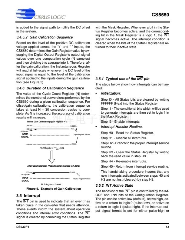
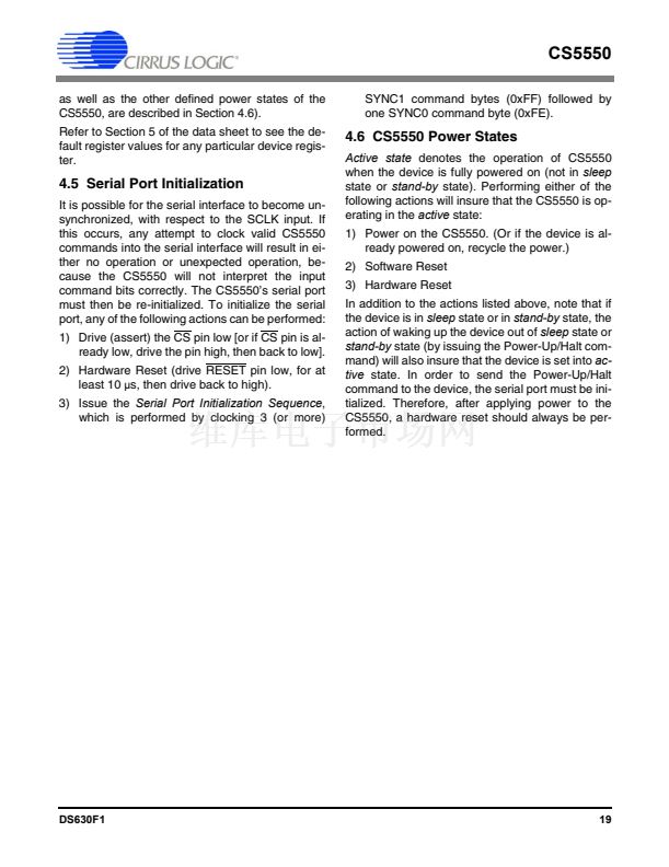
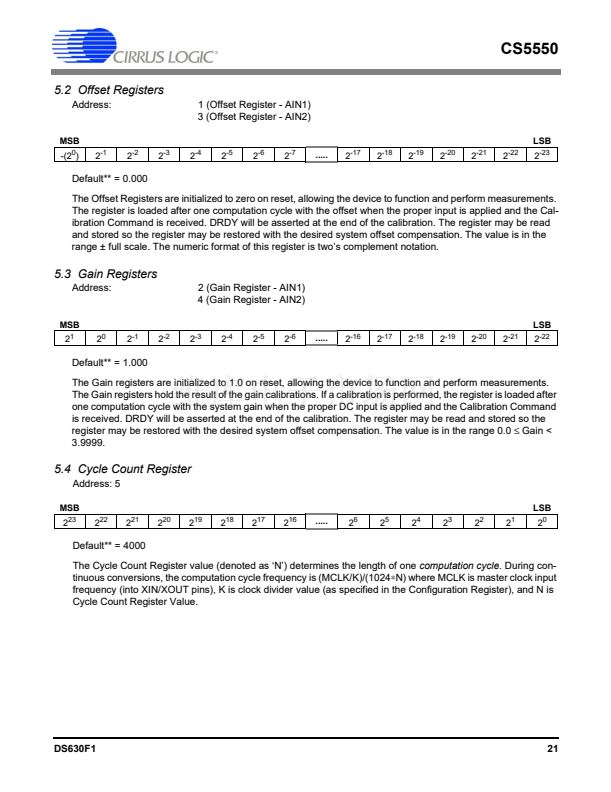
3.4.5.2 Gain Calibration Sequence
Based on the level of the positive DC calibration
voltage applied across the 鈥?鈥?and 鈥?鈥?inputs, the
CS5550 determines the Gain Register value by av-
eraging the Digital Output Register鈥檚 output signal
values over one computation cycle (N samples)
and then dividing this average into 1. Therefore, af-
ter the gain calibration, the Instantaneous Register
will read at full-scale whenever the DC level of the
input signal is equal to the level of the calibration
signal applied to the inputs during the gain calibra-
tion (see Figure 5).
3.5.1 Typical use of the INT pin
The steps below show how interrupts can be han-
dled.
3.4.6 Duration of Calibration Sequence
The value of the Cycle Count Register (N) deter-
mines the number of conversions performed by the
CS5550 during a given calibration sequence. For
offset/gain calibrations, the calibration sequence
takes at least N + 30 conversion cycles to com-
plete. As N is increased, the accuracy of calibration
results will increase.
Before Gain Calibration (Vgain Register = 1)
250 mV
230 mV
DC Signal
鈥?/div>
Initialization:
Step I0 - All Status bits are cleared by writing
FFFFFF (Hex) into the Status Register.
Step I1 - The conditional bits which will be used
to generate interrupts are then set to logic 1 in
the Mask Register.
Step I3 - Enable interrupts.
0.9999...
0.92
Output Register Values
鈥?/div>
Interrupt Handler Routine:
Step H0 - Read the Status Register.
Step H1 - Disable all interrupts.
Step H2 - Branch to the proper interrupt service
routine.
Step H3 - Clear the Status Register by writing
back the read value in step H0.
Step H4 - Re-enable interrupts.
INPUT
0 V
SIGNAL
-250 mV
-1.0000...
FILT Register =
230
/
250
=
0.92
After Gain Calibration (Vgain Register changed to 1.0870)
230 mV
DC Signal
Step H5 - Return from interrupt service routine.
This handshaking procedure insures that any
new interrupts activated between steps H0 and
H3 are not lost (cleared) by step H3.
0.9999...
Ouptut Register Values
INPUT
0 V
SIGNAL
FILT Register = 0.9999...
3.5.2 INT Active State
The behavior of the INT pin is controlled by the IM-
ODE and IINV bits of the Configuration Register.
The pin can be active low (default), active high, ac-
tive on a return to logic 0 (pulse-low), or active on
a return to logic 1 (pulse-high). If the interrupt out-
put signal format is set for either pulse-high or
Figure 5. Example of Gain Calibration
3.5 Interrupt
The INT pin is used to indicate that an event has
taken place in the converter that needs attention.
These events inform the system about operation
conditions and internal error conditions. The INT
signal is created by combining the Status Register
DS630F1
13


 1
1
 2
2
 3
3
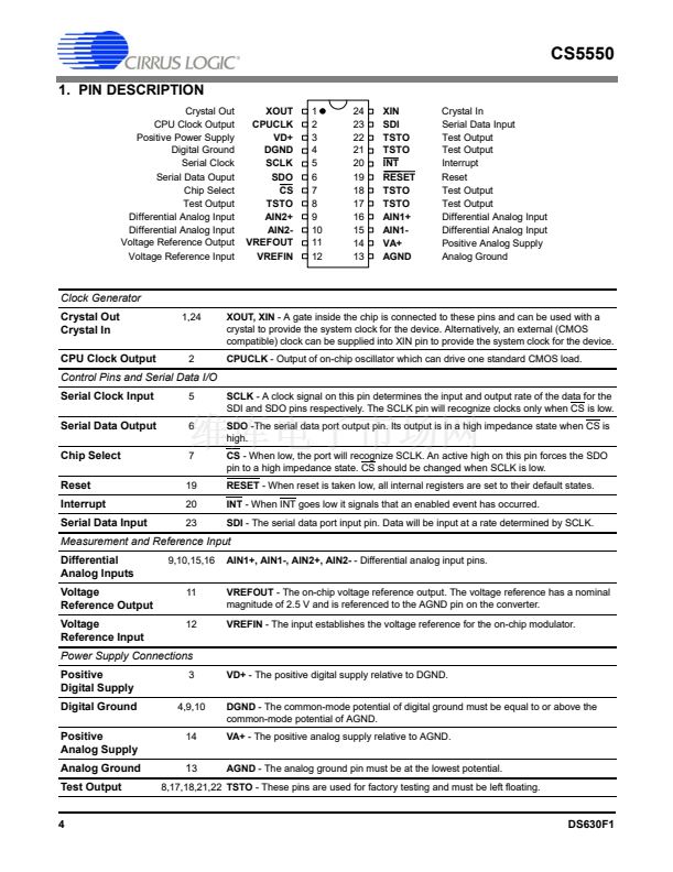 4
4
 5
5
 6
6
 7
7
 8
8
 9
9
 10
10
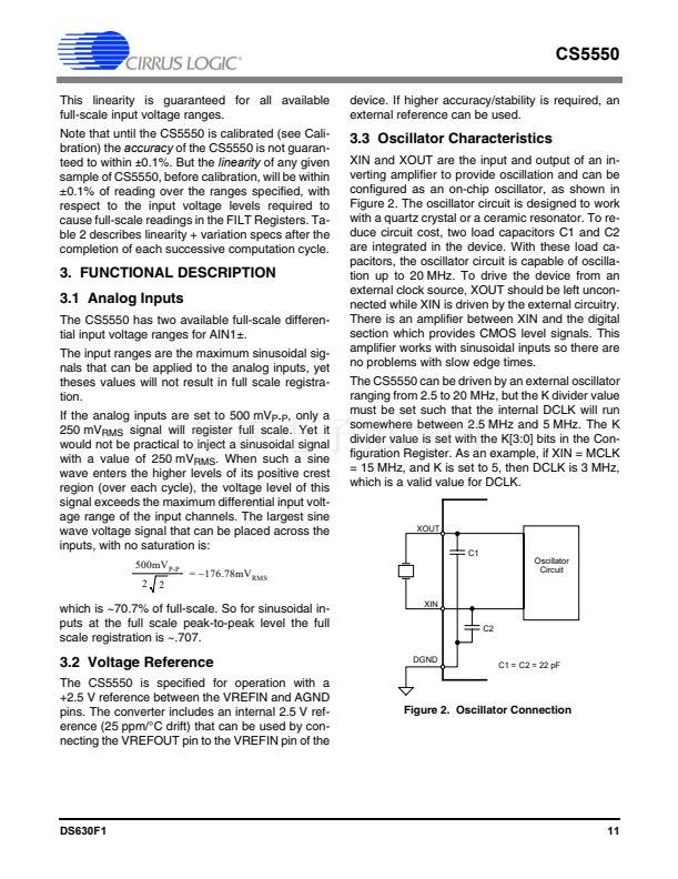 11
11
 12
12
 13
13
 14
14
 15
15
 16
16
 17
17
 18
18
 19
19
 20
20
 21
21
 22
22
 23
23
 24
24
