鈥?/div>
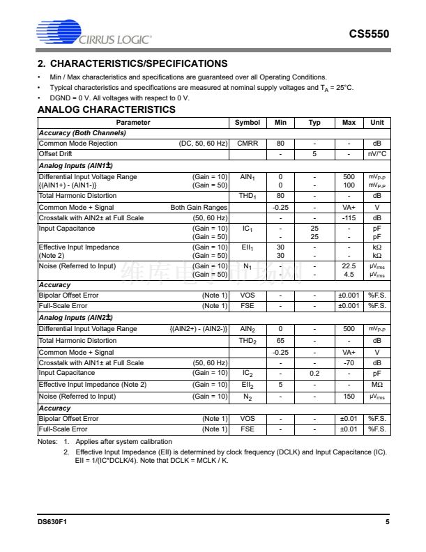
Min / Max characteristics and specifications are guaranteed over all Operating Conditions.
Typical characteristics and specifications are measured at nominal supply voltages and T
A
= 25掳C.
DGND = 0 V. All voltages with respect to 0 V.
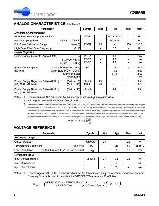
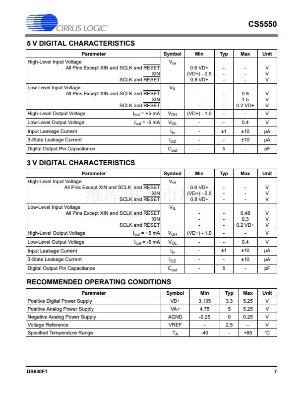
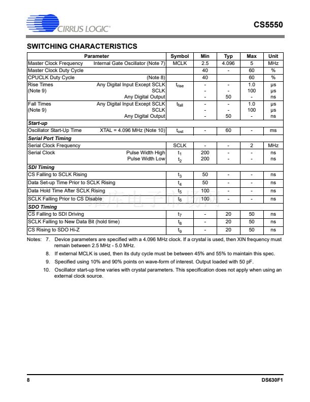
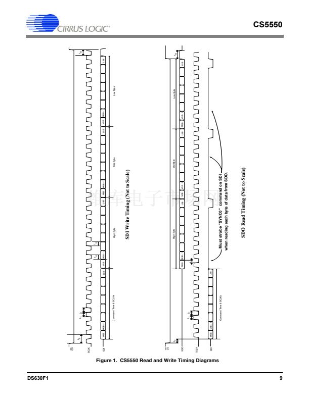
ANALOG CHARACTERISTICS
Parameter
Accuracy (Both Channels)
Common Mode Rejection
Offset Drift
Analog Inputs (AIN1
卤
)
Differential Input Voltage Range
{(AIN1+) - (AIN1-)}
Total Harmonic Distortion
Common Mode + Signal
Crosstalk with AIN2卤 at Full Scale
Input Capacitance
Effective Input Impedance
(Note 2)
Noise (Referred to Input)
Accuracy
Bipolar Offset Error
Full-Scale Error
Analog Inputs (AIN2
卤
)
Differential Input Voltage Range
Total Harmonic Distortion
Common Mode + Signal
Crosstalk with AIN1卤 at Full Scale
Input Capacitance
Effective Input Impedance (Note 2)
Noise (Referred to Input)
Accuracy
Bipolar Offset Error
Full-Scale Error
Notes: 1. Applies after system calibration
2. Effective Input Impedance (EII) is determined by clock frequency (DCLK) and Input Capacitance (IC).
EII = 1/(IC*DCLK/4). Note that DCLK = MCLK / K.
(Note 1)
(Note 1)
VOS
FSE
-
-
-
-
卤0.01
卤0.01
%F.S.
%F.S.
(50, 60 Hz)
(Gain = 10)
(Gain = 10)
(Gain = 10)
IC
2
EII
2
N
2
{(AIN2+) - (AIN2-)}
AIN
2
THD
2
0
65
-0.25
-
-
5
-
-
-
-
-
0.2
-
-
500
-
VA+
-70
-
-
150
mV
P-P
Symbol
(DC, 50, 60 Hz)
CMRR
Min
80
-
Typ
-
5
-
-
-
-
-
25
25
-
-
-
-
-
-
Max
-
-
500
100
-
VA+
-115
-
-
-
-
22.5
4.5
卤0.001
卤0.001
Unit
dB
nV/掳C
mV
P-P
mV
P-P
(Gain = 10)
(Gain = 50)
Both Gain Ranges
(50, 60 Hz)
(Gain = 10)
(Gain = 50)
(Gain = 10)
(Gain = 50)
(Gain = 10)
(Gain = 50)
(Note 1)
(Note 1)
AIN
1
THD
1
0
0
80
-0.25
-
dB
V
dB
pF
pF
k鈩?/div>
k鈩?/div>
碌V
rms
碌V
rms
IC
1
EII
1
N
1
-
-
30
30
-
-
-
-
VOS
FSE
%F.S.
%F.S.
dB
V
dB
pF
prev
next


 1
1
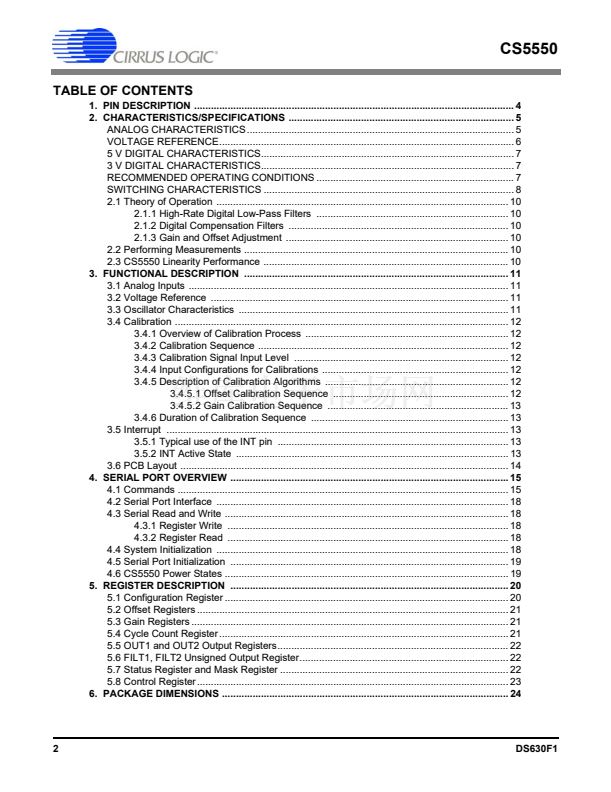 2
2
 3
3
 4
4
 5
5
 6
6
 7
7
 8
8
 9
9
 10
10
 11
11
 12
12
 13
13
 14
14
 15
15
 16
16
 17
17
 18
18
 19
19
 20
20
 21
21
 22
22
 23
23
 24
24
