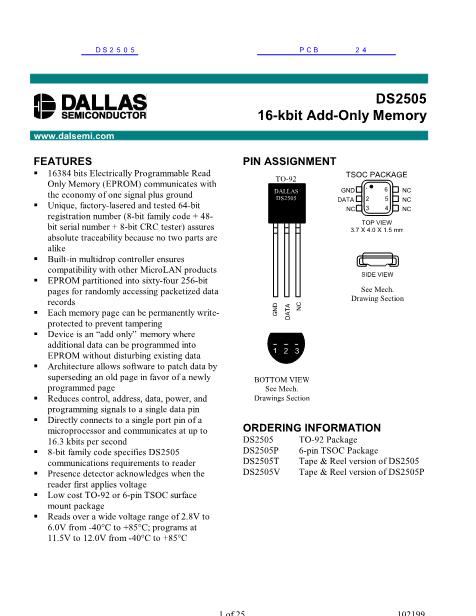
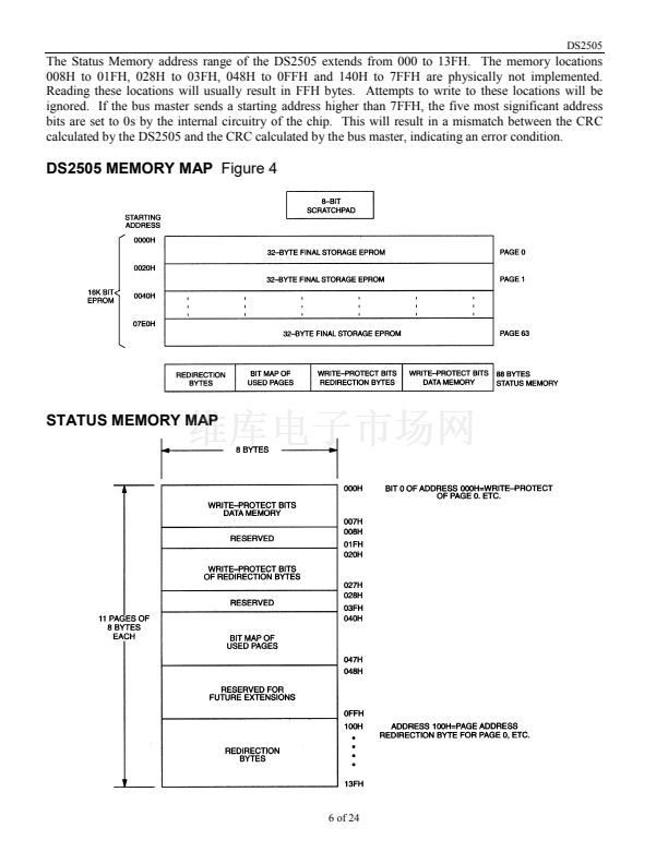
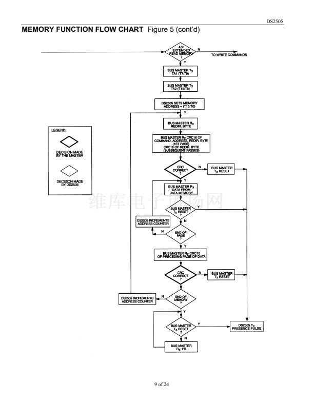
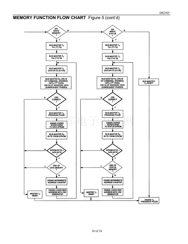
DS2505
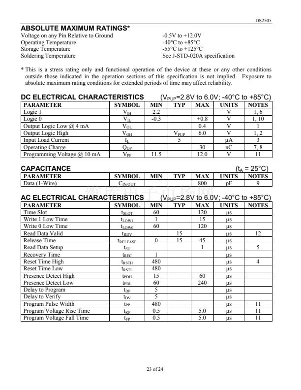
ABSOLUTE MAXIMUM RATINGS*
Voltage on any Pin Relative to Ground
Operating Temperature
Storage Temperature
Soldering Temperature
-0.5V to +12.0V
-40掳C to +85掳C
-55掳C to +125掳C
See J-STD-020A specification
* This is a stress rating only and functional operation of the device at these or any other conditions
outside those indicated in the operation sections of this specification is not implied. Exposure to
absolute maximum rating conditions for extended periods of time may affect reliability.
DC ELECTRICAL CHARACTERISTICS
PARAMETER
Logic 1
Logic 0
Output Logic Low @ 4 mA
Output Logic High
Input Load Current
Operating Charge
Programming Voltage @ 10 mA
SYMBOL
V
IH
V
IL
V
OL
V
OH
I
L
Q
OP
V
PP
(V
PUP
=2.8V to 6.0V; -40掳C to +85掳C)
MIN
2.2
-0.3
TYP
MAX
+0.8
0.4
6.0
30
12.0
UNITS
V
V
V
V
碌A
nC
V
NOTES
1, 6
1, 10
1
1, 2
3
7, 8
11
V
PUP
5
11.5
CAPACITANCE
PARAMETER
Data (1-Wire)
SYMBOL
C
IN/OUT
MIN
TYP
MAX
800
(t
A
= 25掳C)
UNITS
pF
NOTES
9
AC ELECTRICAL CHARACTERISTICS
PARAMETER
Time Slot
Write 1 Low Time
Write 0 Low Time
Read Data Valid
Release Time
Read Data Setup
Recovery Time
Reset Time High
Reset Time Low
Presence Detect High
Presence Detect Low
Delay to Program
Delay to Verify
Program Pulse Width
Program Voltage Rise Time
Program Voltage Fall Time
SYMBOL
t
SLOT
t
LOW1
t
LOW0
t
RDV
t
RELEASE
t
SU
t
REC
t
RSTH
t
RSTL
t
PDH
t
PDL
t
DP
t
DV
t
PP
t
RP
t
FP
(V
PUP
=2.8V to 6.0V; -40掳C to +85掳C)
MIN
60
1
60
0
1
480
480
15
60
5
5
480
0.5
0.5
TYP
MAX
120
15
120
45
1
UNITS
碌s
碌s
碌s
碌s
碌s
碌s
碌s
碌s
碌s
碌s
碌s
碌s
碌s
碌s
碌s
碌s
NOTES
15
15
12
5
4
60
240
5.0
5.0
11
11
11
23 of 24


 1
1
 2
2
 3
3
 4
4
 5
5
 6
6
 7
7
 8
8
 9
9
 10
10
 11
11
 12
12
 13
13
 14
14
 15
15
 16
16
 17
17
 18
18
 19
19
 20
20
 21
21
 22
22
 23
23
 24
24
