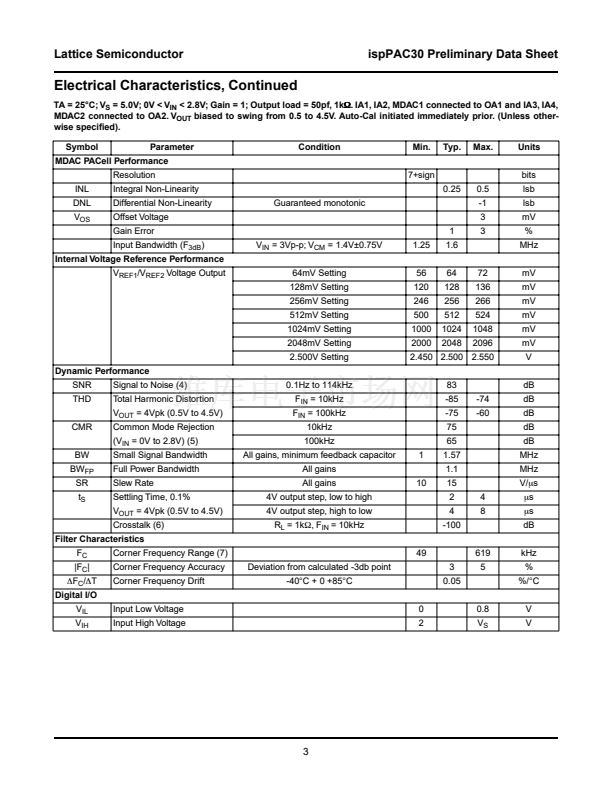
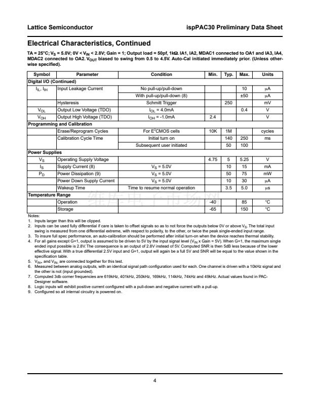
Lattice Semiconductor
ispPAC30 Preliminary Data Sheet
Theory of Operation
General Description
The ispPAC30 provides programmable, multiple single-ended or differential signal inputs, precision gain, offset
adjustment, 铿乴tering, and comparison functionality all in a single device. It also has complete routability of inputs or
outputs to any input cell and then to either summing node of the internal output ampli铿乪rs. A key feature of the
ispPAC30 is its capability of being recon铿乬ured in real time, apart from the operation of its non-volatile E
2
CMOS or
E
2
con铿乬uration memory. This enables the user to change or recon铿乬ure the ispPAC30 an unlimited number of
times, such as in an automatic gain control circuit or other applications requiring ongoing parametric or routing
changes. Because a user chosen con铿乬uration is always stored in non-volatile E
2
con铿乬uration memory as well,
there is a preset con铿乬uration ready to go when the device is 铿乺st turned on, or whenever a return to that stored
state is required. Of course, the E
2
con铿乬uration can be updated at any time during normal device operation as a
completely transparent background operation. All of this functionality and 铿俥xibility is combined into the ispPAC30
as a single integrated circuit that greatly simpli铿乪s the otherwise burdensome task of designing and customizing
circuitry for a wide variety of analog applications.
The following sections of this data sheet give the user a thorough understanding of the general operation and
design considerations necessary when using the ispPAC30. Another resource that cannot be overlooked for under-
standing the ispPAC30 is associated with the PAC-Designer software design tool. Everything that can be con铿乬-
ured is accessible in a schematic entry based format. A complete appreciation of the ispPAC30鈥檚 capabilities is
enhanced by exploring and using this design software early to learn more about it. Because a simulator is included,
the user can quickly test and prove operational modes and arrive at an understanding sooner while exploring
device capabilities. Complete documentation of PAC-Designer is included with the software.
Further technical insight into the ispPAC30 can be gained by referring to the many application notes and circuit
solutions that directly relate to this device. All ispPAC technical support literature is available from the Lattice Semi-
conductor web site at www.latticesemi.com. In addition, Lattice provides expert applications support for all ispPAC
devices and their usage.
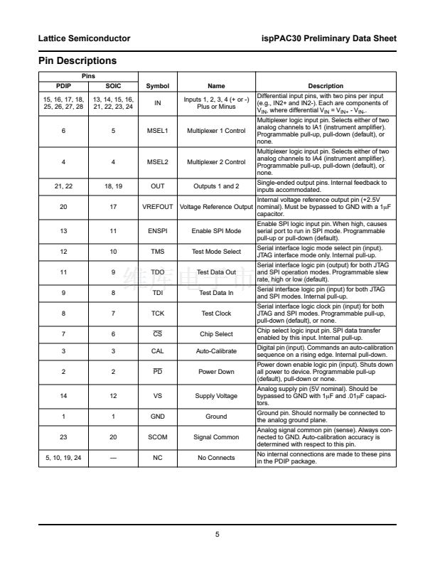
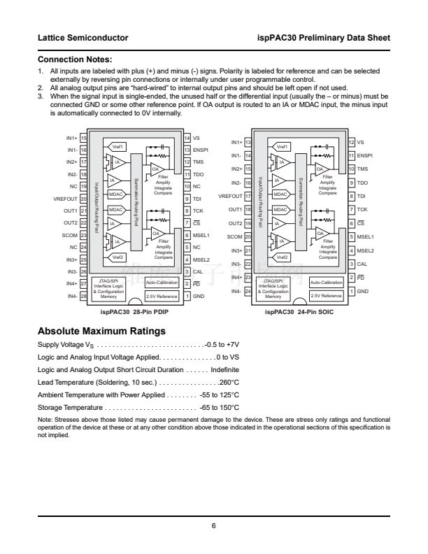
Device Input Cells
In an ispPAC30 device, any input pin can be routed to any of the four input instrument ampli铿乪rs (IA), two of which
have dual input multiplexers, or to either of the two multiplying DAC鈥檚 (MDAC), or any combination of these. In addi-
tion, either output ampli铿乪r (OA) can be routed to any or all of these same input cells. This enables great 铿俥xibility
in how an ispPAC30 is con铿乬ured and allows many functions to be performed, such as signal summation, cas-
caded gain blocks, complex feedback circuits, etc.
At the ispPAC30 input pins, the input signal range that can be directly applied is 0 to 2.8V. When used differentially,
the input pins can be of any polarity with respect to each other as long as the resultant signal is not expected to
drive the OA outputs below 0V. Normally, input signals will be single ended, in which case the
minus input pin
(V
IN-
)
can be tied to ground. Even with single ended measurements, the ispPAC30鈥檚 differential architecture can be used
to an advantage as it will sense ground at the point where it is connected and will also reject any noise common to
both ground and the input signal. Input impedances at all input nodes are the same as would be expected for MOS-
FET devices, and are typically in the Giga-Ohm range. Refer to the speci铿乧ations section for more detail.
Input Instrument Ampli铿乪rs
The input ampli铿乪rs (IA鈥檚) are referred to as instrument ampli铿乪rs because they take the difference of the two input
pins and multiply it by the gain setting for which they have been con铿乬ured. With respect to true differential opera-
tion, this means that a negative gain setting is merely a reversal of the plus and minus input (V
IN
) pins. This is the
classical instrument ampli铿乪r function and also includes the previously mentioned bene铿乼 of remote sensing of sig-
nals (not necessarily 0V referenced) and rejection of common mode signals. Both IA鈥檚 and MDAC鈥檚 connected to
input signals also serve to buffer inputs by virtue of their very high input impedance.
13


 1
1
 2
2
 3
3
 4
4
 5
5
 6
6
 7
7
 8
8
 9
9
 10
10
 11
11
 12
12
 13
13
 14
14
 15
15
 16
16
 17
17
 18
18
 19
19
 20
20
 21
21
 22
22
 23
23
 24
24
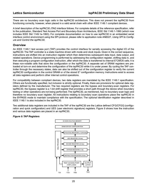 25
25
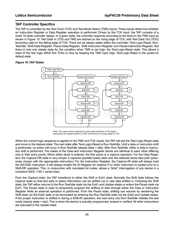 26
26
 27
27
 28
28
 29
29
 30
30
