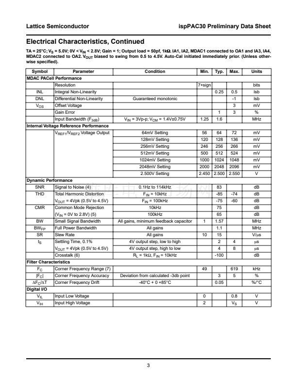
鈩?/div>
. IA1, IA2, MDAC1 connected to OA1 and IA3, IA4,
MDAC2 connected to OA2. V
OUT
biased to swing from 0.5 to 4.5V. Auto-Cal initiated immediately prior. (Unless other-
wise speci铿乪d).
Symbol
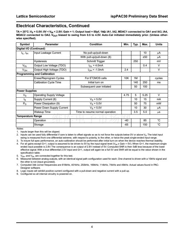
Digital I/O (Continued)
I
IL
, I
IH
Input Leakage Current
Hysteresis
V
OL
V
OH
Output Low Voltage (TDO)
Output High Voltage (TDO)
Erase/Reprogram Cycles
Calibration Cycle Time
Power Supplies
V
S
I
S
P
D
Operating Supply Voltage
Supply Current (8)
Power Dissipation (9)
Power Down Supply Current
Wakeup Time
Temperature Range
Operation
Storage
-40
-65
85
150
掳C
掳C
V
S
= 5.0V
V
S
= 5.0V
V
S
= 5.0V
Time to resume normal operation
4.75
5
10
50
10
3.5
5.25
15
75
30
5.0
V
mA
mW
碌A
碌s
No pull-up/pull-down
With pull-up/pull-down (8)
Schmitt Trigger
I
OL
= 4.0mA
I
OH
= -1.0mA
For E
2
CMOS cells
Initial turn on
Subsequent user initiated
2.4
10K
1M
140
50
250
100
250
0.4
10
卤50
碌A
碌
A
mV
V
V
cycles
ms
Parameter
Condition
Min.
Typ.
Max.
Units
Programming and Calibration
Notes:
1. Inputs larger than this will be clipped.
2. Inputs can be used fully differential if care is taken to offset signals so as to not force the outputs below 0V or above V
S
. The total input
swing is measured from one differential extreme, with respect to polarity, to the other, or twice the peak single-ended input range.
3. To insure full spec performance, an auto-calibration should be performed after initial turn-on when the device reaches thermal stability.
4. For all gains except G=1, output is assumed to be driven to 5V by the input signal level (V
IN
x Gain = 5V). When G=1, the maximum single
ended input possible is 2.8V. The consequence is an output of 2.8V instead of 5V. Computed SNR is then 5dB less because of the lower
effective signal. With a true differential 2.5V input and G=1, output will again be a full 5V and SNR will be equal to the value shown in the
speci铿乧ation table.
5. V
IN+
and V
IN-
are connected together for this test.
6. Measured between analog outputs, with an identical signal path con铿乬uration used for each. One channel is driven with a 10kHz signal and
the other is not (input grounded).
7. Computed 3db corner frequencies are 619kHz, 401kHz, 250kHz, 169kHz, 114kHz, 74kHz and 49kHz. Actual values found in PAC-
Designer software.
8. Logic inputs will exhibit positive current con铿乬ured with a pull-down and negative current with a pull-up.
9. Con铿乬ured so all internal circuitry is powered on.
4


 1
1
 2
2
 3
3
 4
4
 5
5
 6
6
 7
7
 8
8
 9
9
 10
10
 11
11
 12
12
 13
13
 14
14
 15
15
 16
16
 17
17
 18
18
 19
19
 20
20
 21
21
 22
22
 23
23
 24
24
 25
25
 26
26
 27
27
 28
28
 29
29
 30
30
