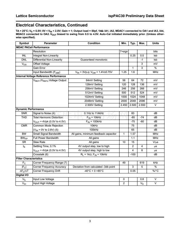
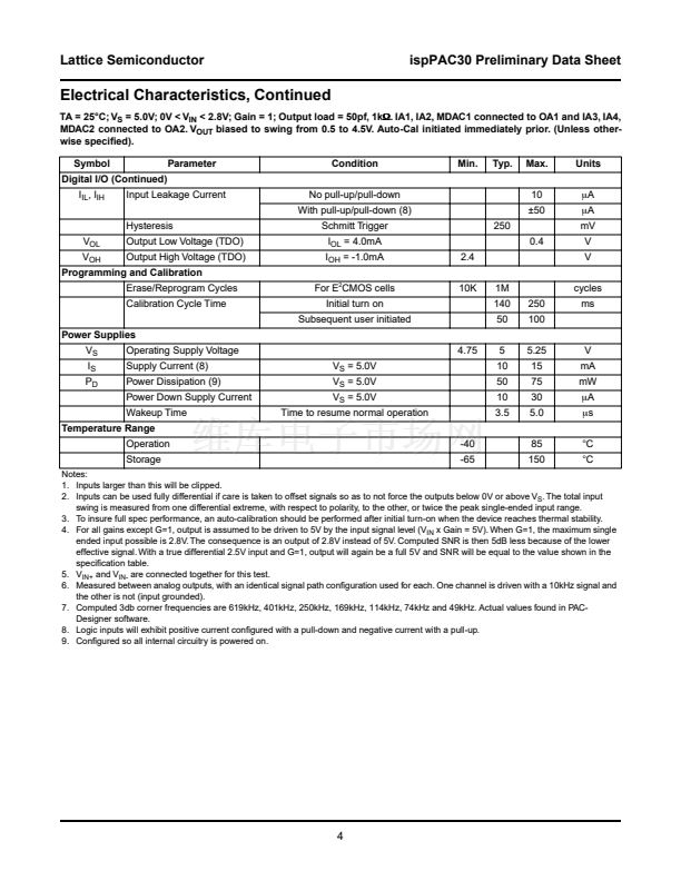
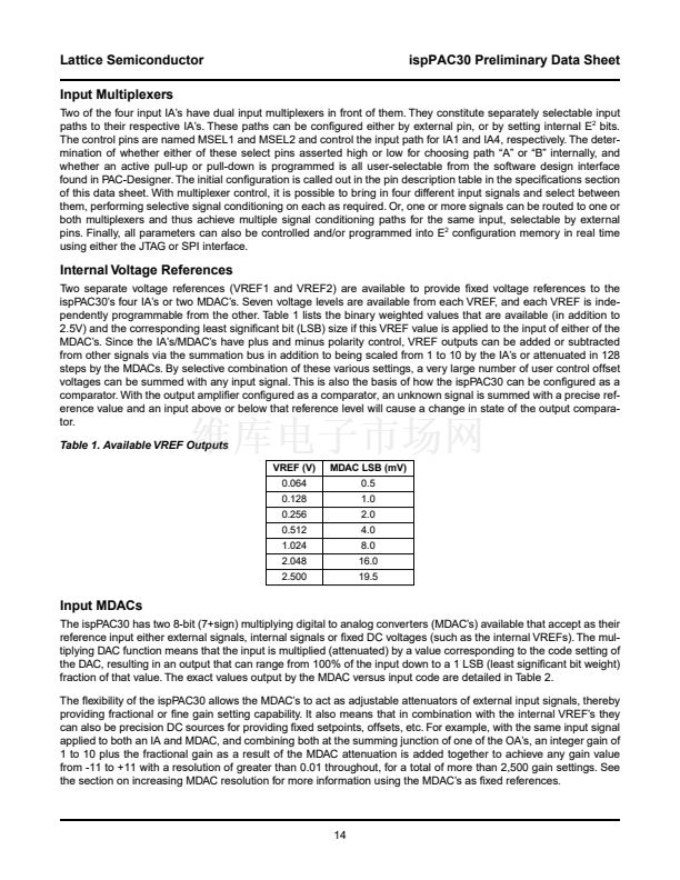
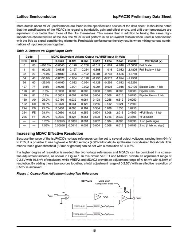
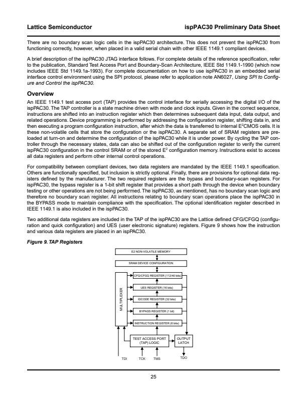
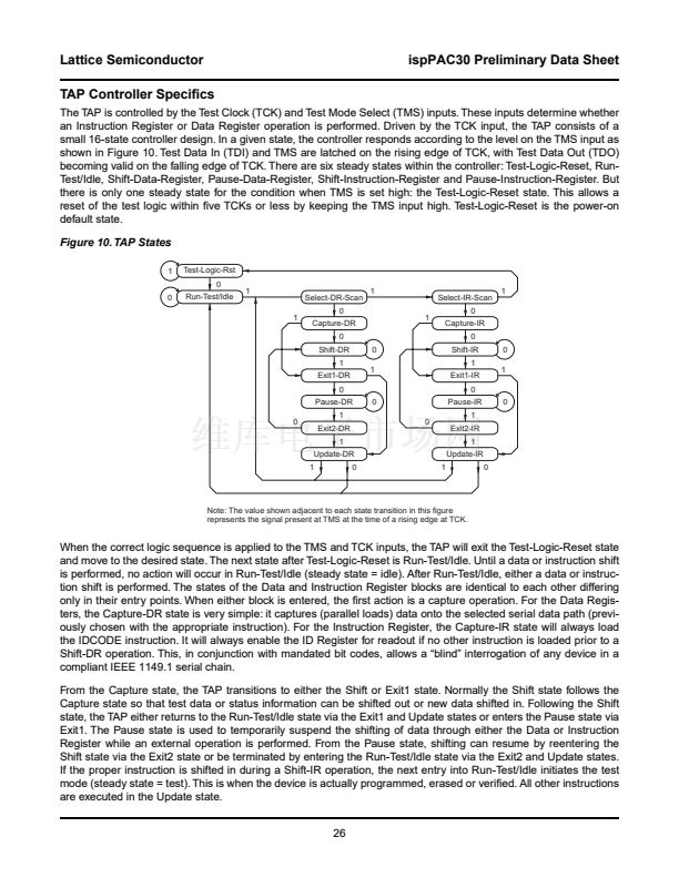
Lattice Semiconductor
ispPAC30 Preliminary Data Sheet
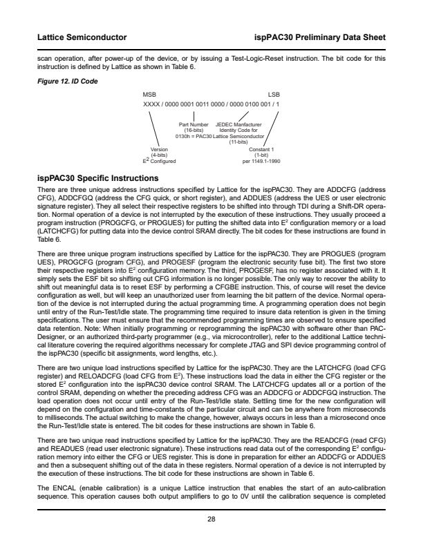
scan operation, after power-up of the device, or by issuing a Test-Logic-Reset instruction. The bit code for this
instruction is de铿乶ed by Lattice as shown in Table 6.
Figure 12. ID Code
MSB
LSB
XXXX / 0000 0001 0011 0000 / 0000 0100 001 / 1
Part Number JEDEC Manfacturer
(16-bits)
Identity Code for
0130h = PAC30 Lattice Semiconductor
(11-bits)
Version
Constant 1
(4-bits)
(1-bit)
per 1149.1-1990
E 2 Configured
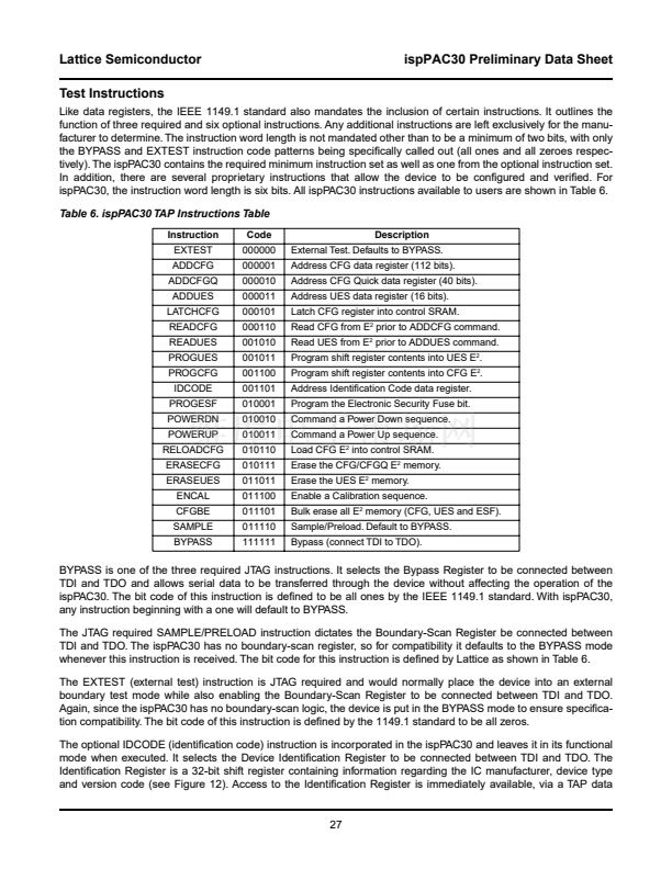
ispPAC30 Speci铿乧 Instructions
There are three unique address instructions speci铿乪d by Lattice for the ispPAC30. They are ADDCFG (address
CFG), ADDCFGQ (address the CFG quick, or short register), and ADDUES (address the UES or user electronic
signature register). They all select their respective registers to be shifted into through TDI during a Shift-DR opera-
tion. Normal operation of a device is not interrupted by the execution of these instructions. They usually proceed a
program instruction (PROGCFG, or PROGUES) for putting the shifted data into E
2
con铿乬uration memory or a load
(LATCHCFG) for putting data into the device control SRAM directly. The bit codes for these instructions are found in
Table 6.
There are three unique program instructions speci铿乪d by Lattice for the ispPAC30. They are PROGUES (program
UES), PROGCFG (program CFG), and PROGESF (program the electronic security fuse bit). The 铿乺st two store
their respective registers into E
2
con铿乬uration memory. The third, PROGESF, has no register associated with it. It
simply sets the ESF bit so shifting out CFG information is no longer possible. The only way to recover the ability to
shift out meaningful data is to reset ESF by performing a CFGBE instruction. This, of course will reset the device
con铿乬uration as well, but will keep an unauthorized user from learning the bit pattern of the device. Normal opera-
tion of the device is not interrupted during the actual programming time. A programming operation does not begin
until entry of the Run-Test/Idle state. The programming time required to insure data retention is given in the timing
speci铿乧ations. The user must ensure that the recommended programming times are observed to ensure speci铿乪d
data retention. Note: When initially programming or reprogramming the ispPAC30 with software other than PAC-
Designer, or an authorized third-party programmer (e.g., via microcontroller), refer to the additional Lattice techni-
cal literature covering the required algorithms necessary for complete JTAG and SPI device programming control of
the ispPAC30 (speci铿乧 bit assignments, word lengths, etc.).
There are two unique load instructions speci铿乪d by Lattice for the ispPAC30. They are the LATCHCFG (load CFG
register) and RELOADCFG (load CFG from E
2
). These instructions load the data in either the CFG register or the
stored E
2
con铿乬uration into the ispPAC30 device control SRAM. The LATCHCFG updates all or a portion of the
control SRAM, depending on whether the preceding address CFG was an ADDCFG or ADDCFGQ instruction. The
load operation does not occur until entry of the Run-Test/Idle state. Settling time for the new con铿乬uration will
depend on the con铿乬uration and time-constants of the particular circuit and can be anywhere from microseconds
to milliseconds. The actual switching to make the change, however, always occurs in less than a microsecond once
the Run-Test/Idle state is entered. The bit codes for these instructions are shown in Table 6.
There are two unique read instructions speci铿乪d by Lattice for the ispPAC30. They are the READCFG (read CFG)
and READUES (read user electronic signature). These instructions read data out of the corresponding E
2
con铿乬u-
ration memory into either the CFG or UES register. This is done in preparation for either an ADDCFG or ADDUES
and then a subsequent shifting out of the data in these registers. Normal operation of a device is not interrupted by
the execution of these instructions. The bit code for these instructions are shown in Table 6.
The ENCAL (enable calibration) is a unique Lattice instruction that enables the start of an auto-calibration
sequence. This operation causes both output ampli铿乪rs to go to 0V until the calibration sequence is completed
28


 1
1
 2
2
 3
3
 4
4
 5
5
 6
6
 7
7
 8
8
 9
9
 10
10
 11
11
 12
12
 13
13
 14
14
 15
15
 16
16
 17
17
 18
18
 19
19
 20
20
 21
21
 22
22
 23
23
 24
24
 25
25
 26
26
 27
27
 28
28
 29
29
 30
30
