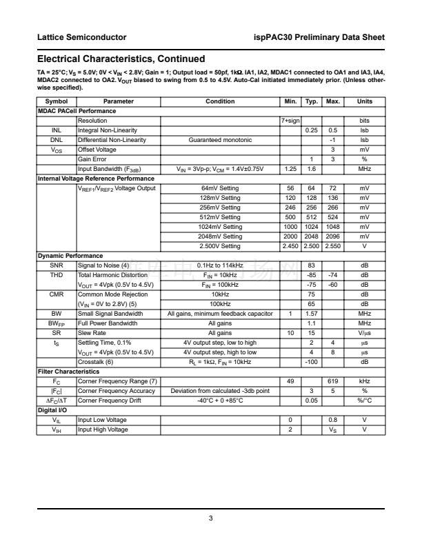
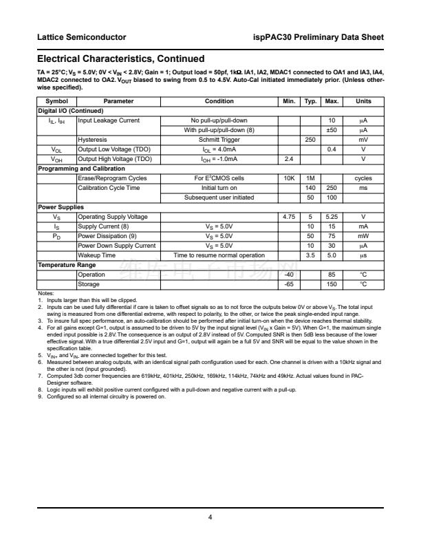
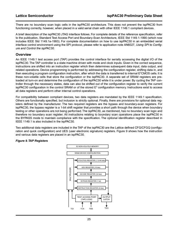
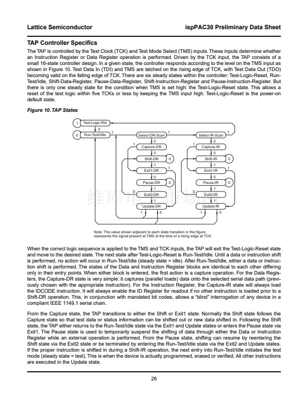
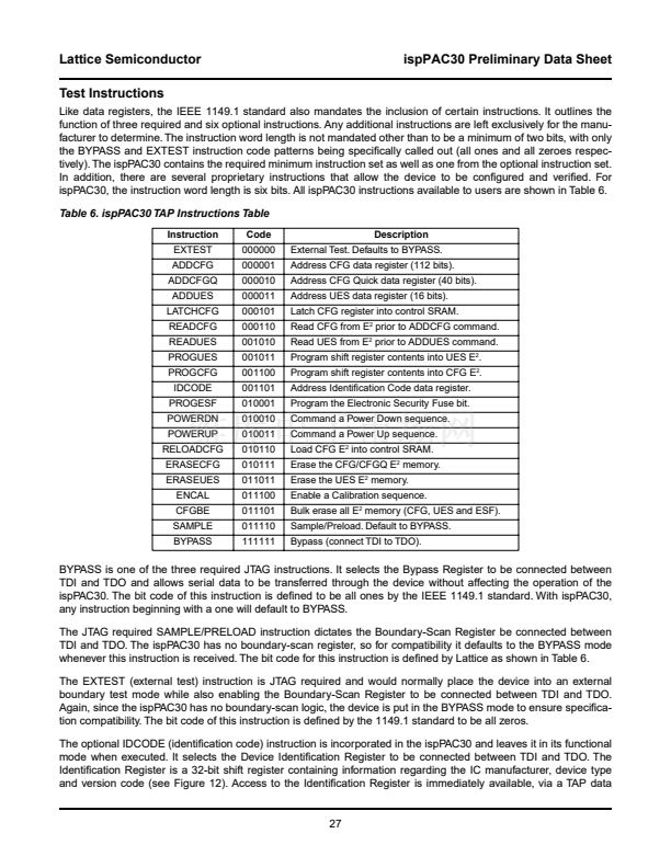
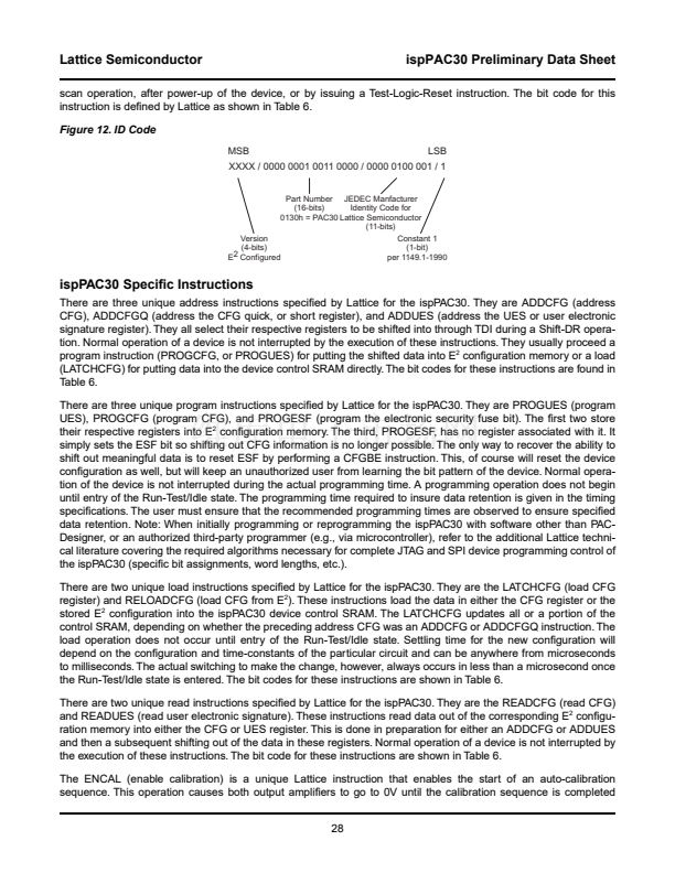
Lattice Semiconductor
Input Multiplexers
ispPAC30 Preliminary Data Sheet
Two of the four input IA鈥檚 have dual input multiplexers in front of them. They constitute separately selectable input
paths to their respective IA鈥檚. These paths can be con铿乬ured either by external pin, or by setting internal E
2
bits.
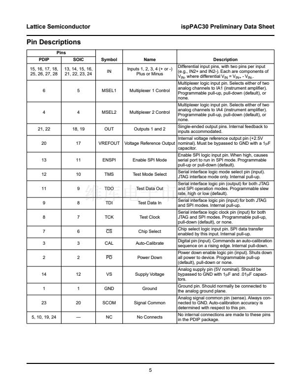
The control pins are named MSEL1 and MSEL2 and control the input path for IA1 and IA4, respectively. The deter-
mination of whether either of these select pins asserted high or low for choosing path 鈥淎鈥?or 鈥淏鈥?internally, and
whether an active pull-up or pull-down is programmed is all user-selectable from the software design interface
found in PAC-Designer. The initial con铿乬uration is called out in the pin description table in the speci铿乧ations section
of this data sheet. With multiplexer control, it is possible to bring in four different input signals and select between
them, performing selective signal conditioning on each as required. Or, one or more signals can be routed to one or
both multiplexers and thus achieve multiple signal conditioning paths for the same input, selectable by external
pins. Finally, all parameters can also be controlled and/or programmed into E
2
con铿乬uration memory in real time
using either the JTAG or SPI interface.
Internal Voltage References
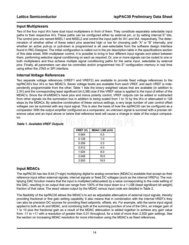
Two separate voltage references (VREF1 and VREF2) are available to provide 铿亁ed voltage references to the
ispPAC30鈥檚 four IA鈥檚 or two MDAC鈥檚. Seven voltage levels are available from each VREF, and each VREF is inde-
pendently programmable from the other. Table 1 lists the binary weighted values that are available (in addition to
2.5V) and the corresponding least signi铿乧ant bit (LSB) size if this VREF value is applied to the input of either of the
MDAC鈥檚. Since the IA鈥檚/MDAC鈥檚 have plus and minus polarity control, VREF outputs can be added or subtracted
from other signals via the summation bus in addition to being scaled from 1 to 10 by the IA鈥檚 or attenuated in 128
steps by the MDACs. By selective combination of these various settings, a very large number of user control offset
voltages can be summed with any input signal. This is also the basis of how the ispPAC30 can be con铿乬ured as a
comparator. With the output ampli铿乪r con铿乬ured as a comparator, an unknown signal is summed with a precise ref-
erence value and an input above or below that reference level will cause a change in state of the output compara-
tor.
Table 1. Available VREF Outputs
VREF (V)
0.064
0.128
0.256
0.512
1.024
2.048
2.500
MDAC LSB (mV)
0.5
1.0
2.0
4.0
8.0
16.0
19.5
Input MDACs
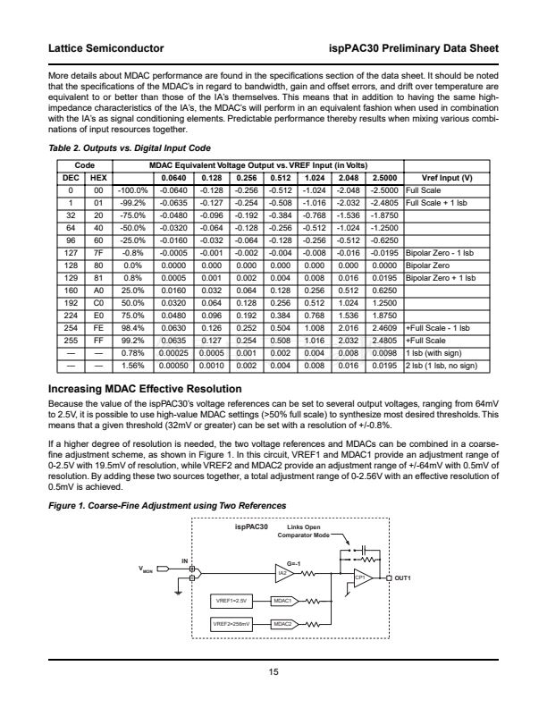
The ispPAC30 has two 8-bit (7+sign) multiplying digital to analog converters (MDAC鈥檚) available that accept as their
reference input either external signals, internal signals or 铿亁ed DC voltages (such as the internal VREFs). The mul-
tiplying DAC function means that the input is multiplied (attenuated) by a value corresponding to the code setting of
the DAC, resulting in an output that can range from 100% of the input down to a 1 LSB (least signi铿乧ant bit weight)
fraction of that value. The exact values output by the MDAC versus input code are detailed in Table 2.
The 铿俥xibility of the ispPAC30 allows the MDAC鈥檚 to act as adjustable attenuators of external input signals, thereby
providing fractional or 铿乶e gain setting capability. It also means that in combination with the internal VREF鈥檚 they
can also be precision DC sources for providing 铿亁ed setpoints, offsets, etc. For example, with the same input signal
applied to both an IA and MDAC, and combining both at the summing junction of one of the OA鈥檚, an integer gain of
1 to 10 plus the fractional gain as a result of the MDAC attenuation is added together to achieve any gain value
from -11 to +11 with a resolution of greater than 0.01 throughout, for a total of more than 2,500 gain settings. See
the section on increasing MDAC resolution for more information using the MDAC鈥檚 as 铿亁ed references.
14


 1
1
 2
2
 3
3
 4
4
 5
5
 6
6
 7
7
 8
8
 9
9
 10
10
 11
11
 12
12
 13
13
 14
14
 15
15
 16
16
 17
17
 18
18
 19
19
 20
20
 21
21
 22
22
 23
23
 24
24
 25
25
 26
26
 27
27
 28
28
 29
29
 30
30
