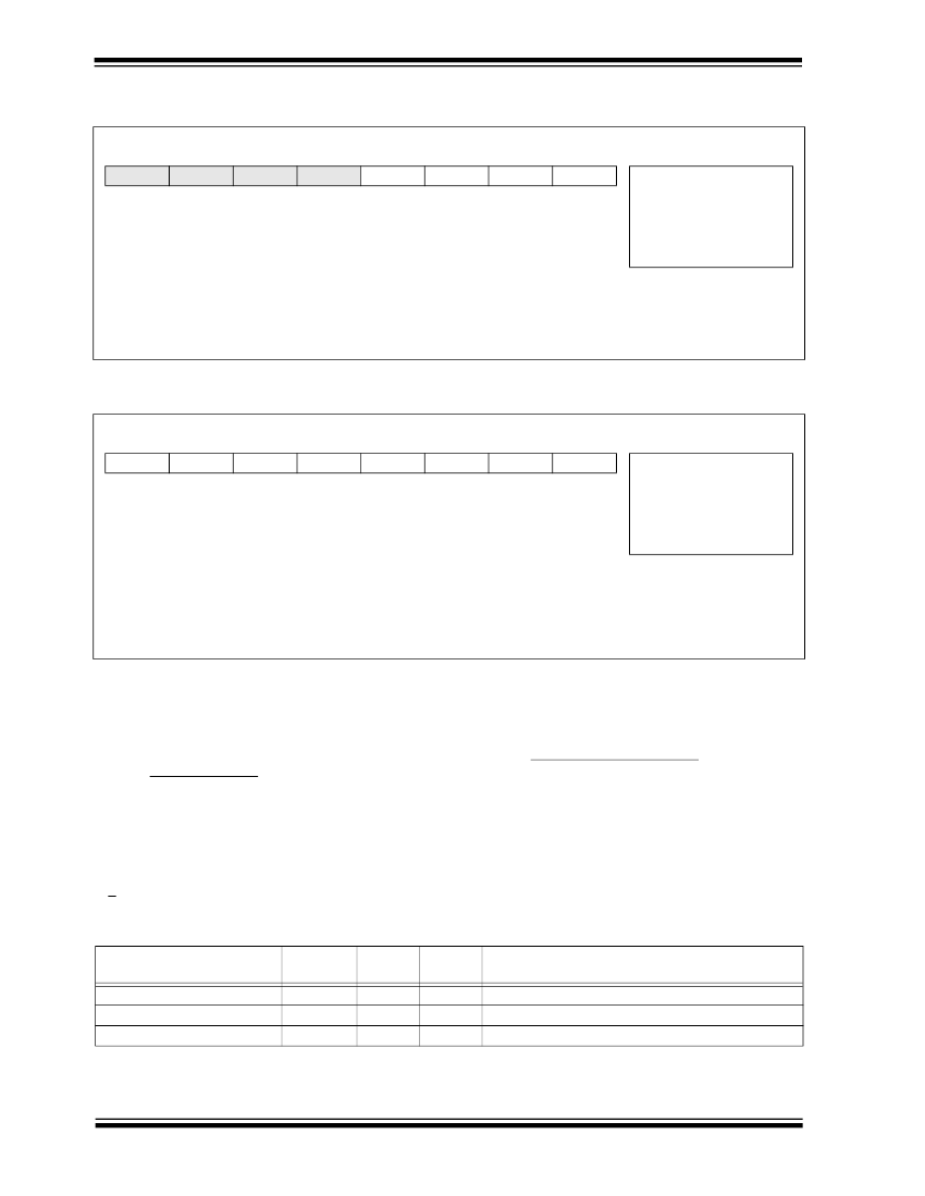
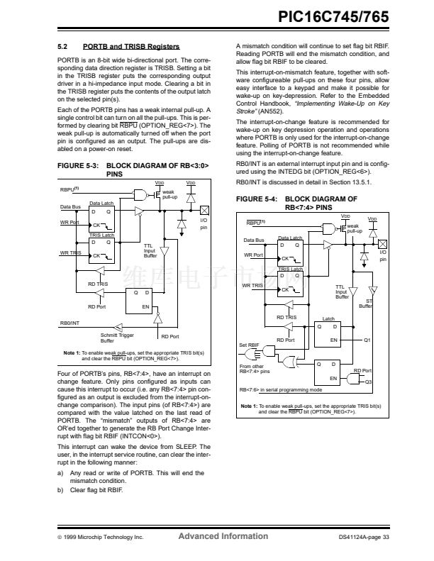
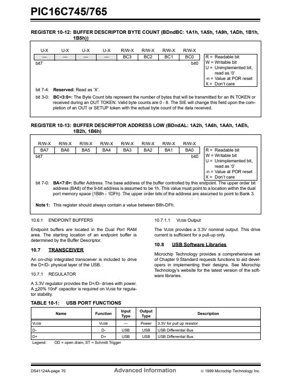
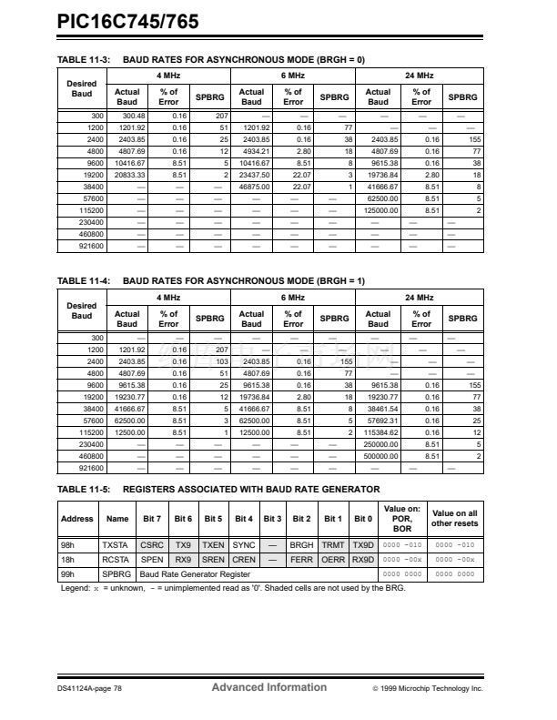
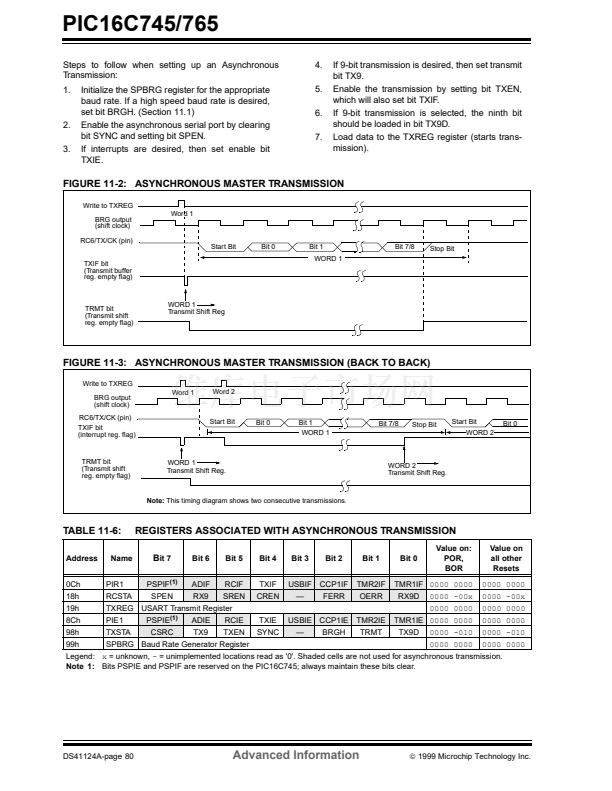
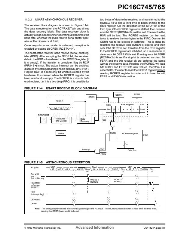
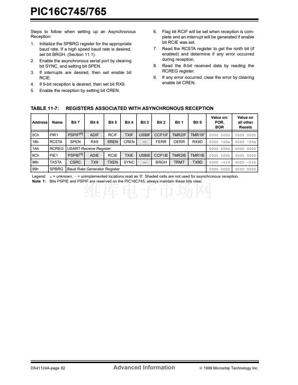
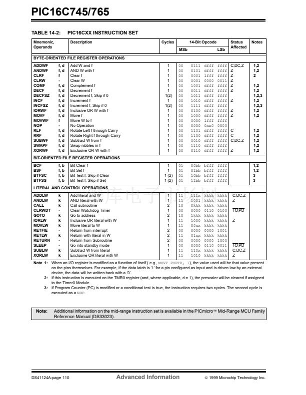
The Byte Count bits represent the number of bytes that will be transmitted for an IN TOKEN or
received during an OUT TOKEN. Valid byte counts are 0 - 8. The SIE will change this field upon the com-
pletion of an OUT or SETUP token with the actual byte count of the data received.
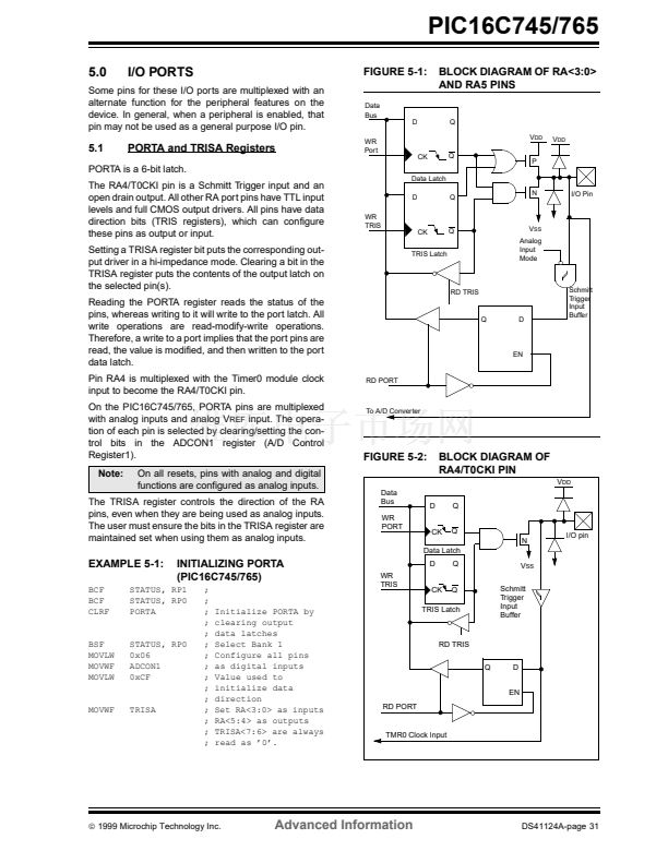
read as 鈥?鈥?/div>
-n = Value at POR reset
X = Don鈥檛 care
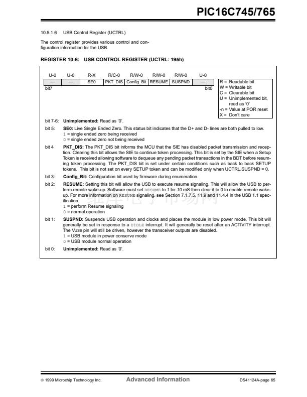
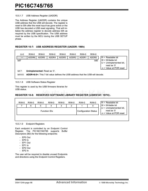
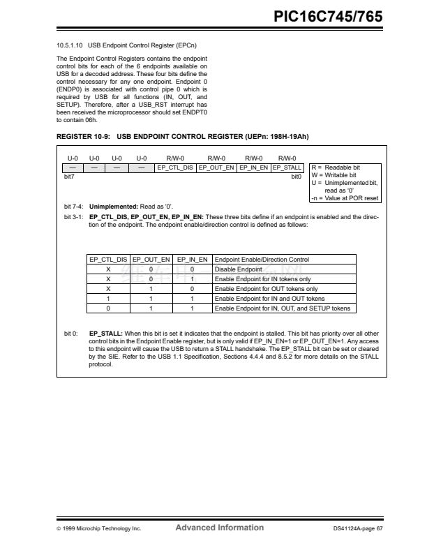
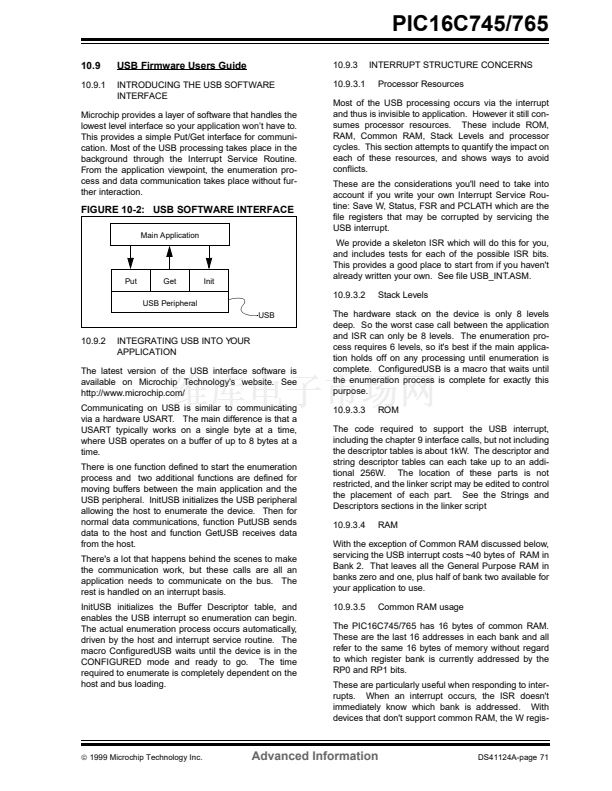
bit 7-0:
BA<7:0>:
Buffer Address. The base address of the buffer controlled by this endpoint. The upper order bit
address (BA8) of the 9-bit address is assumed to be 1h. This value must point to a location within the dual
port memory space (1B8h - 1DFh). The upper order bits of the address are assumed to point to Bank 3.
Note 1:
This register should always contain a value between B8h-DFh.
10.6.1
ENDPOINT BUFFERS
10.7.1.1
V
USB
Output
Endpoint buffers are located in the Dual Port RAM
area. The starting location of an endpoint buffer is
determined by the Buffer Descriptor.
The V
USB
provides a 3.3V nominal output. This drive
current is sufficient for a pull-up only.
10.8
USB Software Libraries
10.7
TRANSCEIVER
An on-chip integrated transceiver is included to drive
the D+/D- physical layer of the USB.
10.7.1
REGULATOR
Microchip Technology provides a comprehensive set
of Chapter 9 Standard requests functions to aid devel-
opers in implementing their designs. See Microchip
Technology鈥檚 website for the latest version of the soft-
ware libraries.
A 3.3V regulator provides the D+/D- drives with power.
A +20% 10nF capacitor is required on V
USB
for regula-
tor stability.
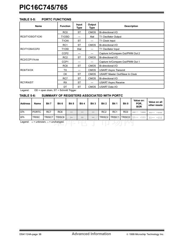
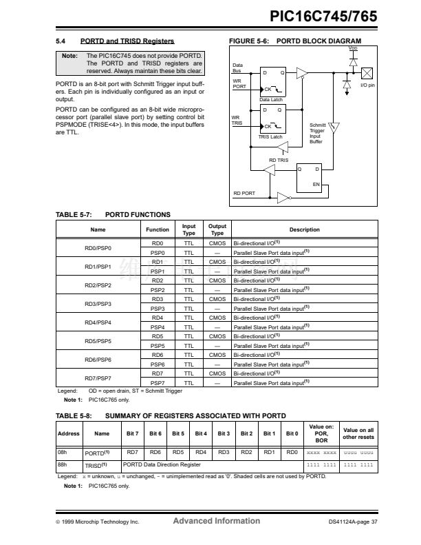
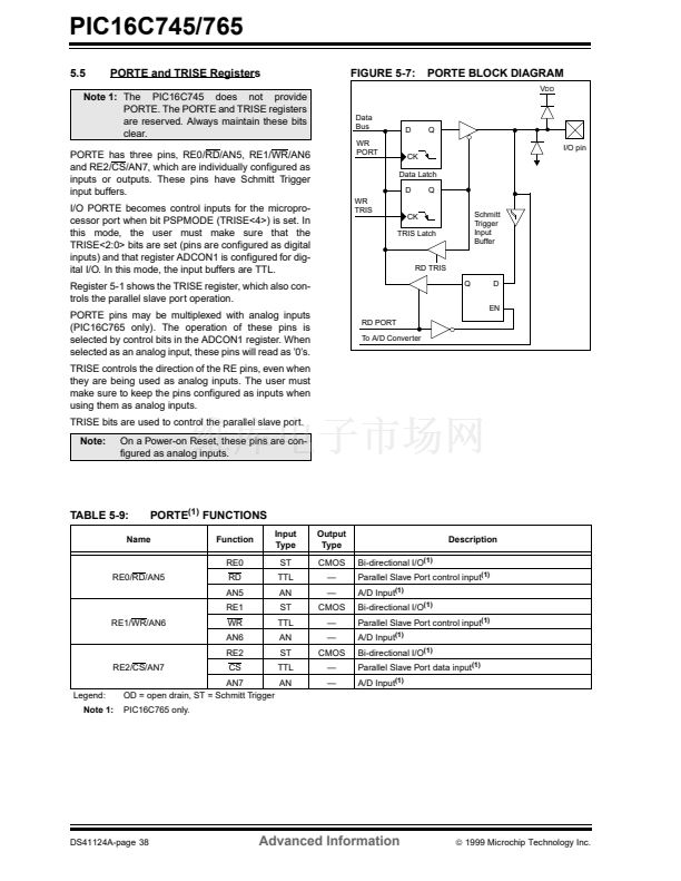
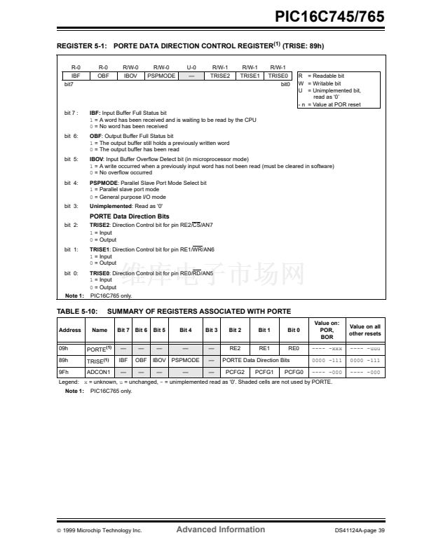
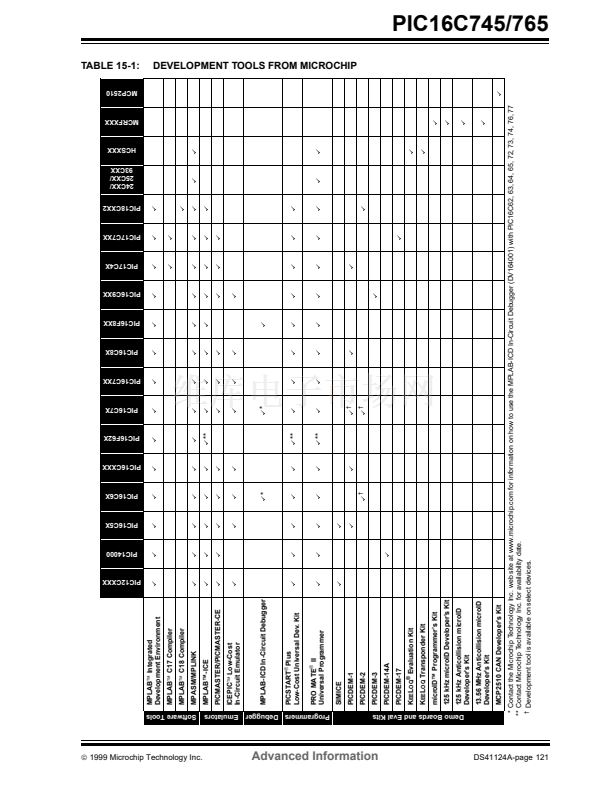
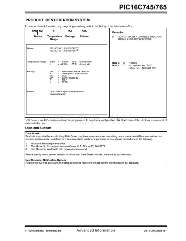
TABLE 10-1:
USB PORT FUNCTIONS
Function
V
USB
D-
Input
Type
鈥?/div>
USB
Output
Type
Power
USB
USB
Description
3.3V for pull up resistor
USB Differential Bus
USB Differential Bus
Name
V
USB
D-
D+
Legend:
D+
USB
OD = open drain, ST = Schmitt Trigger
DS41124A-page 70
Advanced Information
漏
1999 Microchip Technology Inc.


 1
1
 2
2
 3
3
 4
4
 5
5
 6
6
 7
7
 8
8
 9
9
 10
10
 11
11
 12
12
 13
13
 14
14
 15
15
 16
16
 17
17
 18
18
 19
19
 20
20
 21
21
 22
22
 23
23
 24
24
 25
25
 26
26
 27
27
 28
28
 29
29
 30
30
 31
31
 32
32
 33
33
 34
34
 35
35
 36
36
 37
37
 38
38
 39
39
 40
40
 41
41
 42
42
 43
43
 44
44
 45
45
 46
46
 47
47
 48
48
 49
49
 50
50
 51
51
 52
52
 53
53
 54
54
 55
55
 56
56
 57
57
 58
58
 59
59
 60
60
 61
61
 62
62
 63
63
 64
64
 65
65
 66
66
 67
67
 68
68
 69
69
 70
70
 71
71
 72
72
 73
73
 74
74
 75
75
 76
76
 77
77
 78
78
 79
79
 80
80
 81
81
 82
82
 83
83
 84
84
 85
85
 86
86
 87
87
 88
88
 89
89
 90
90
 91
91
 92
92
 93
93
 94
94
 95
95
 96
96
 97
97
 98
98
 99
99
 100
100
 101
101
 102
102
 103
103
 104
104
 105
105
 106
106
 107
107
 108
108
 109
109
 110
110
 111
111
 112
112
 113
113
 114
114
 115
115
 116
116
 117
117
 118
118
 119
119
 120
120
 121
121
 122
122
 123
123
 124
124
 125
125
 126
126
 127
127
 128
128
 129
129
 130
130
 131
131
 132
132
 133
133
 134
134
 135
135
 136
136
 137
137
 138
138
 139
139
 140
140
 141
141
 142
142
 143
143
 144
144
 145
145
 146
146
 147
147
 148
148
 149
149
 150
150
 151
151
 152
152
 153
153
 154
154
 155
155
 156
156
 157
157
 158
158
