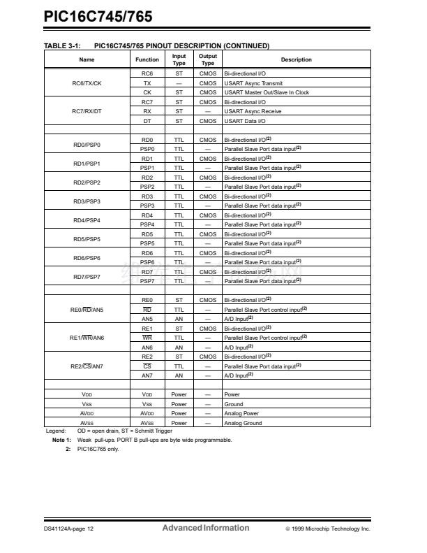
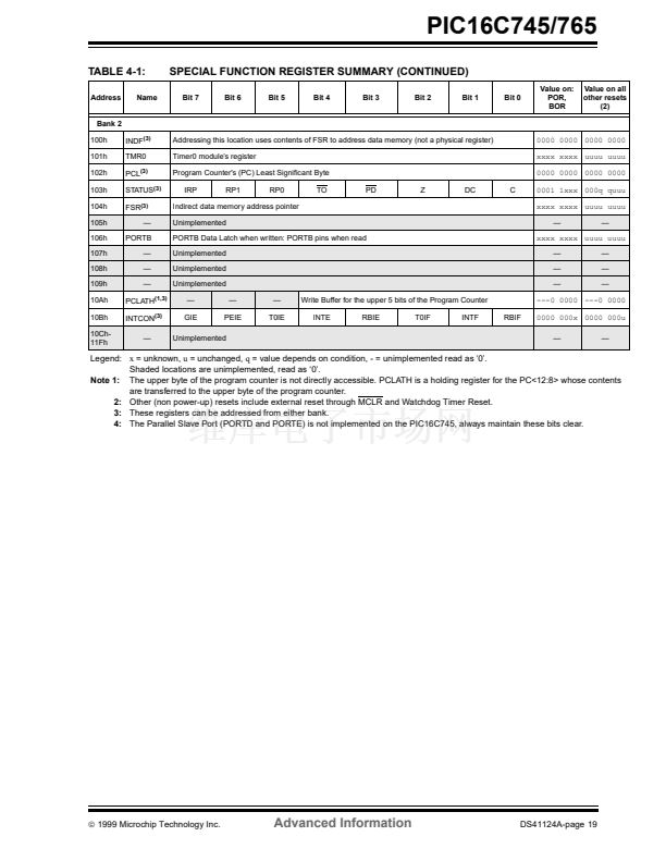
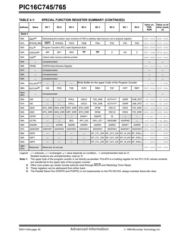
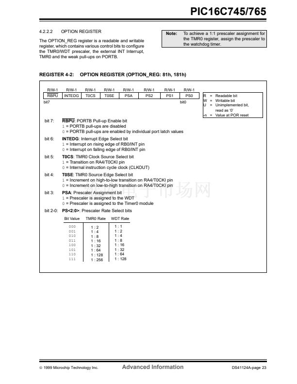
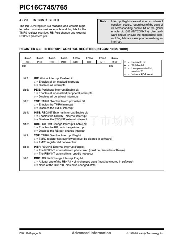
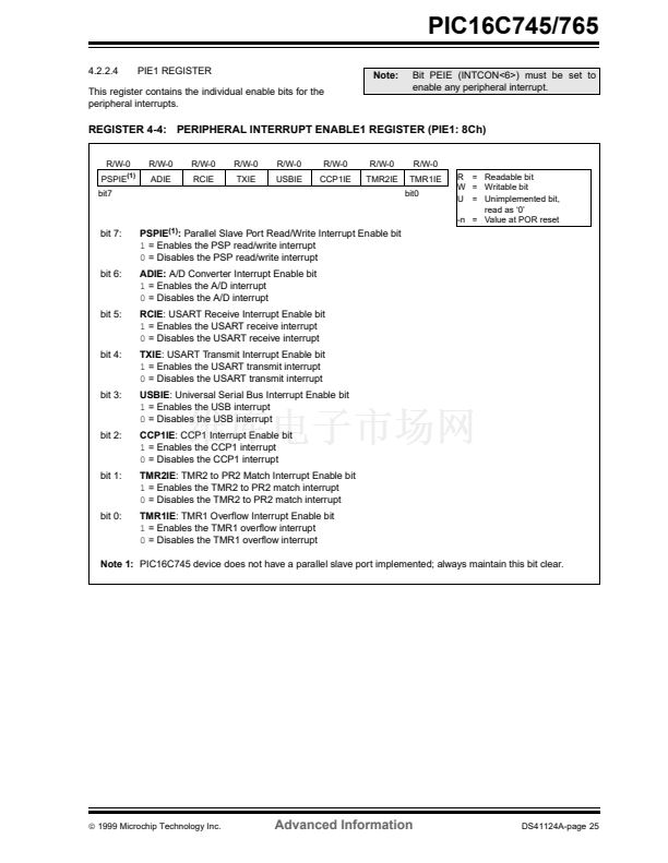
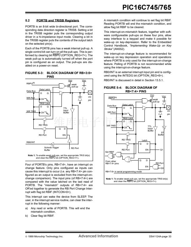
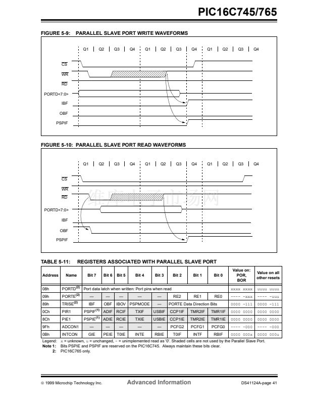
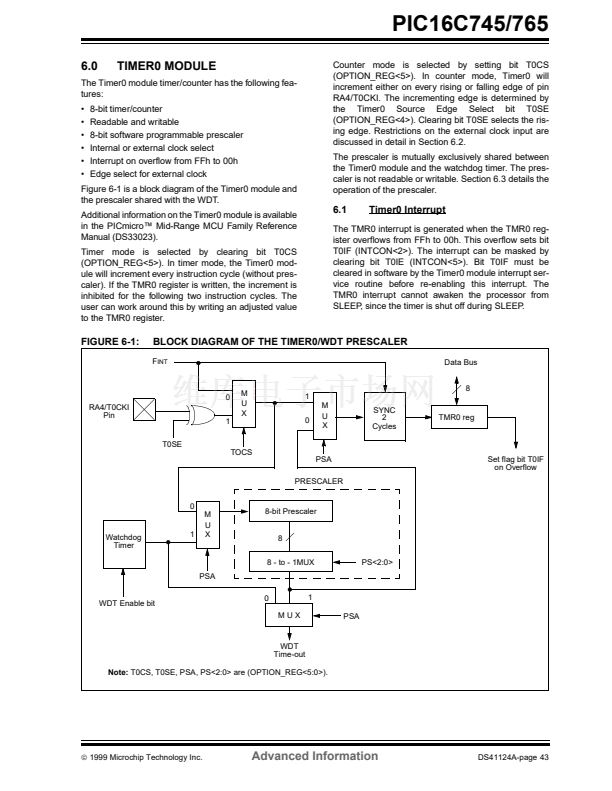
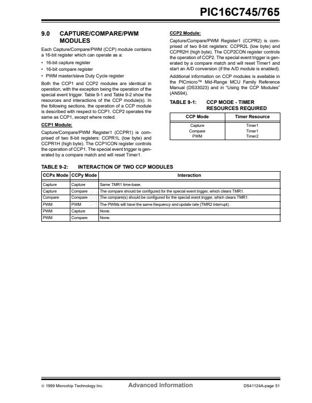
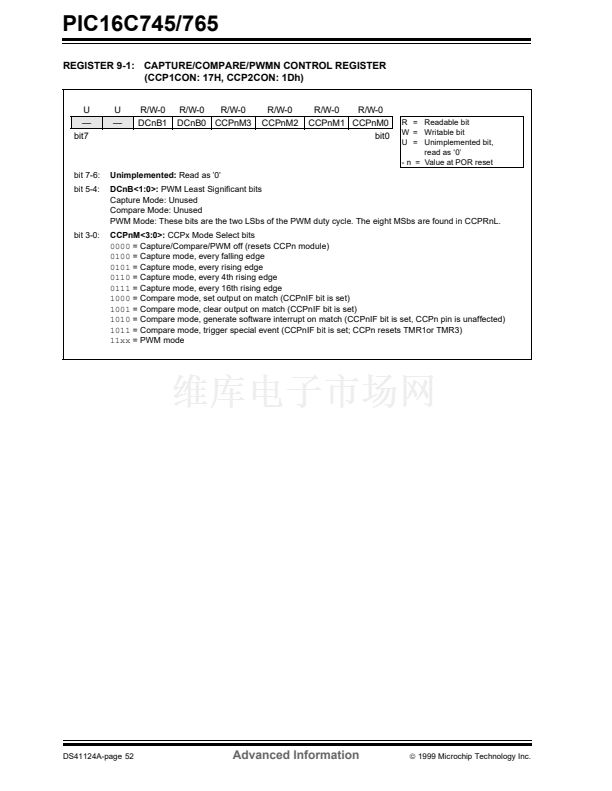
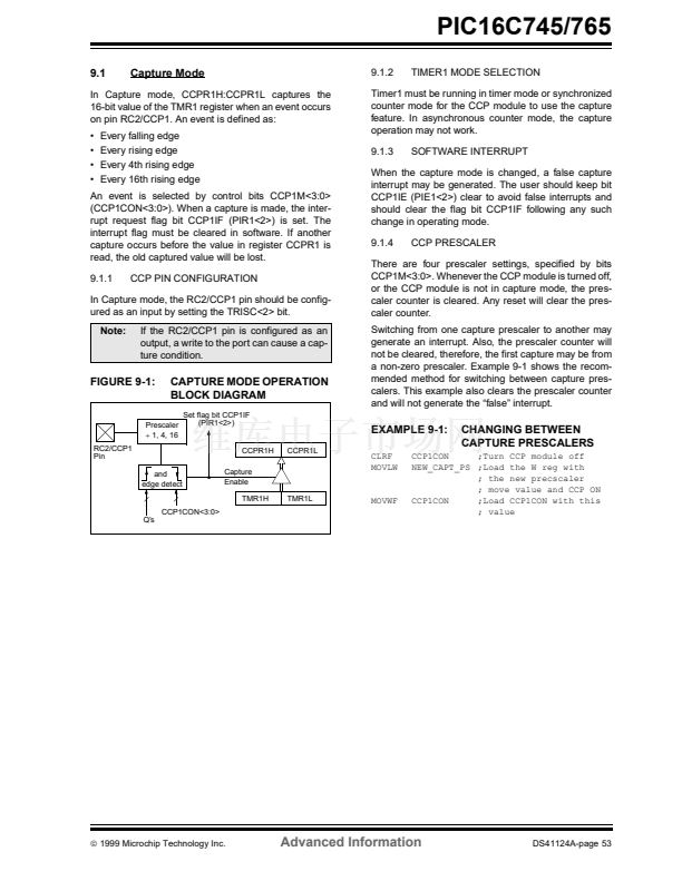
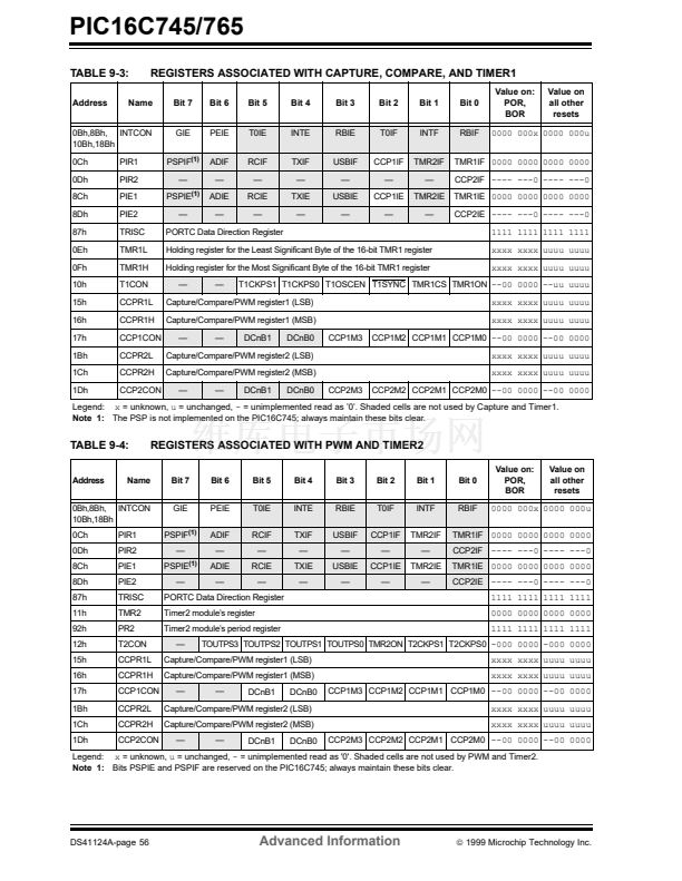
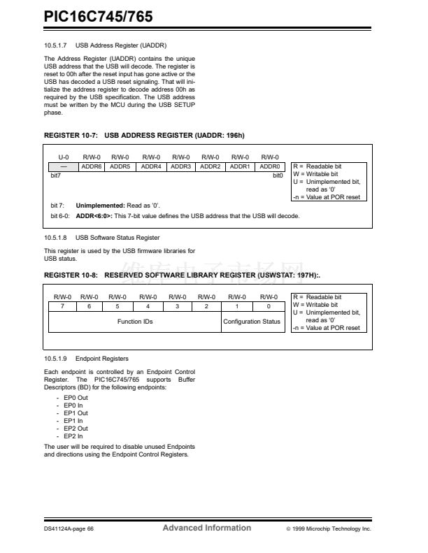
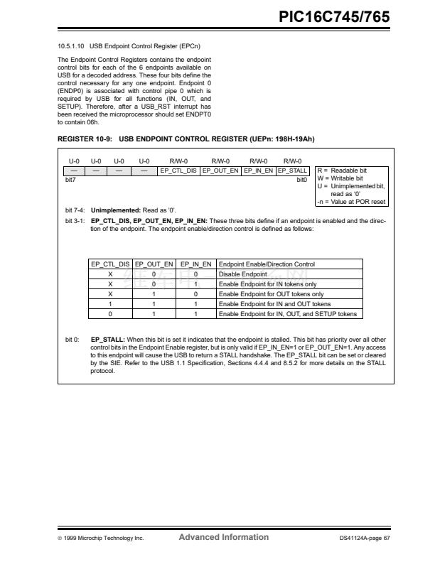
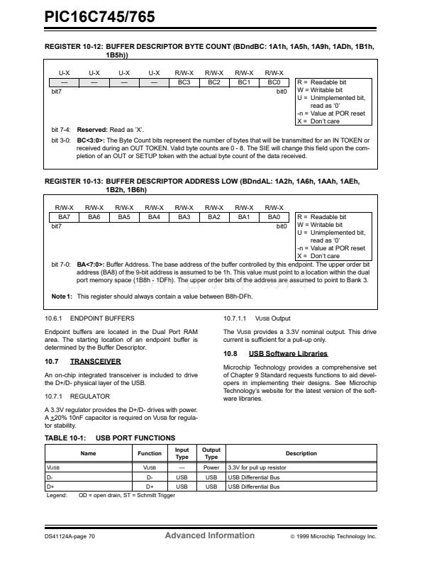
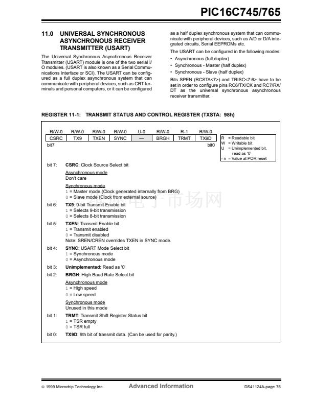
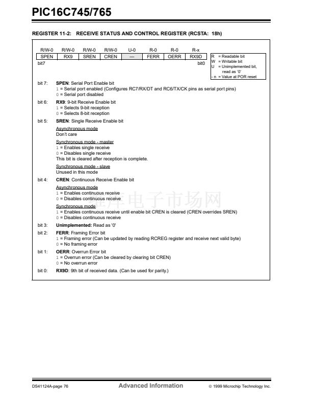
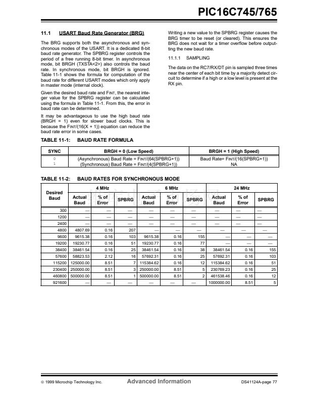
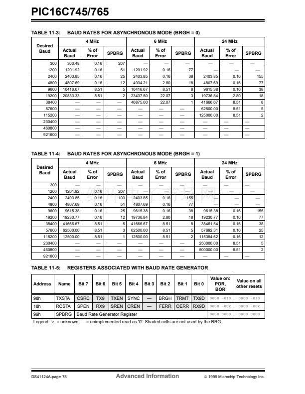
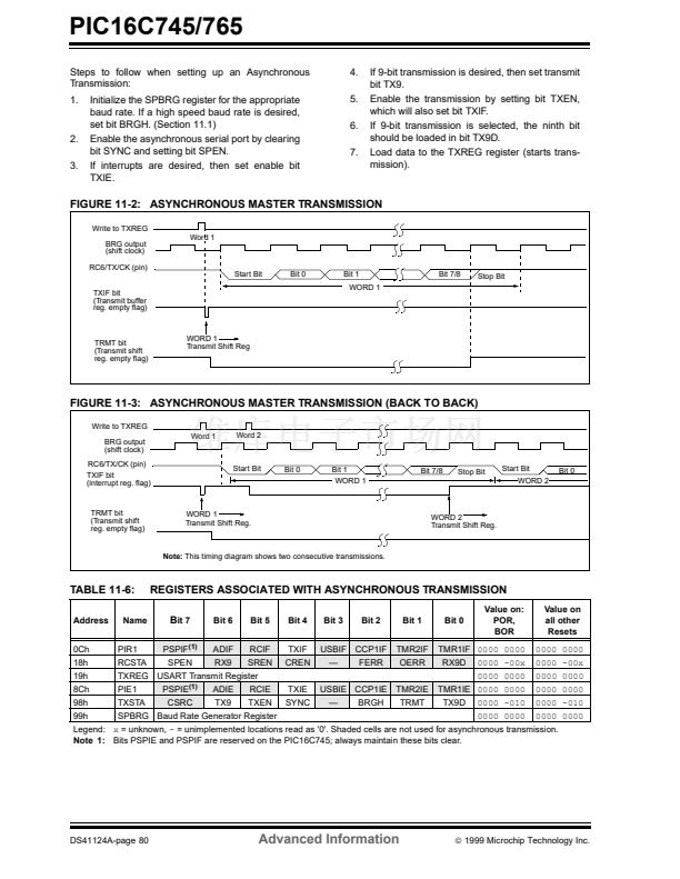
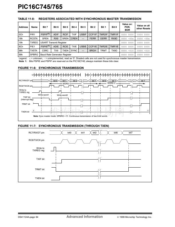
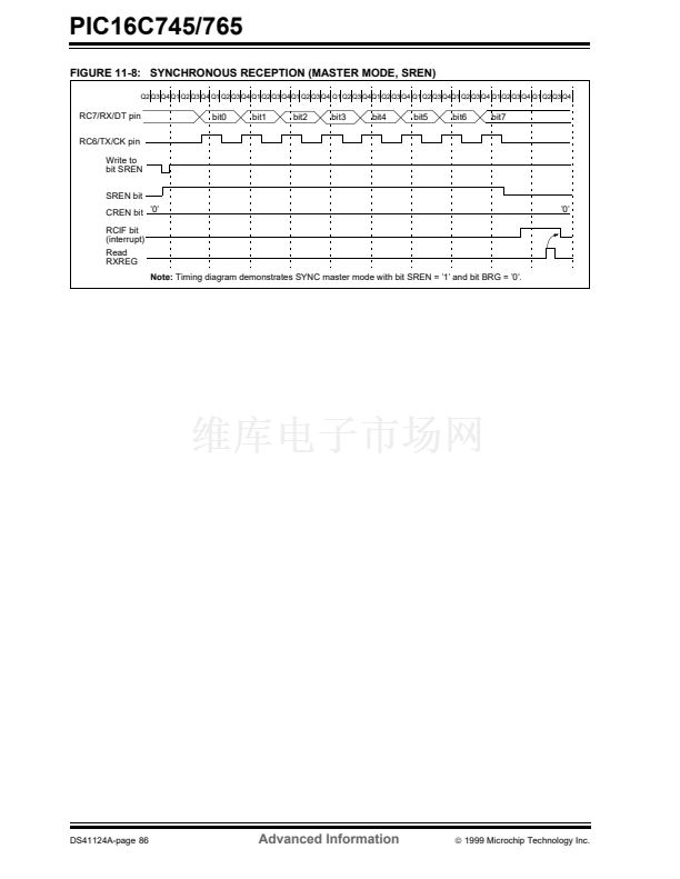
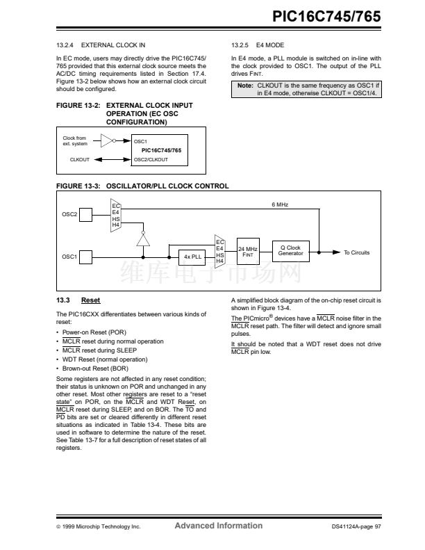
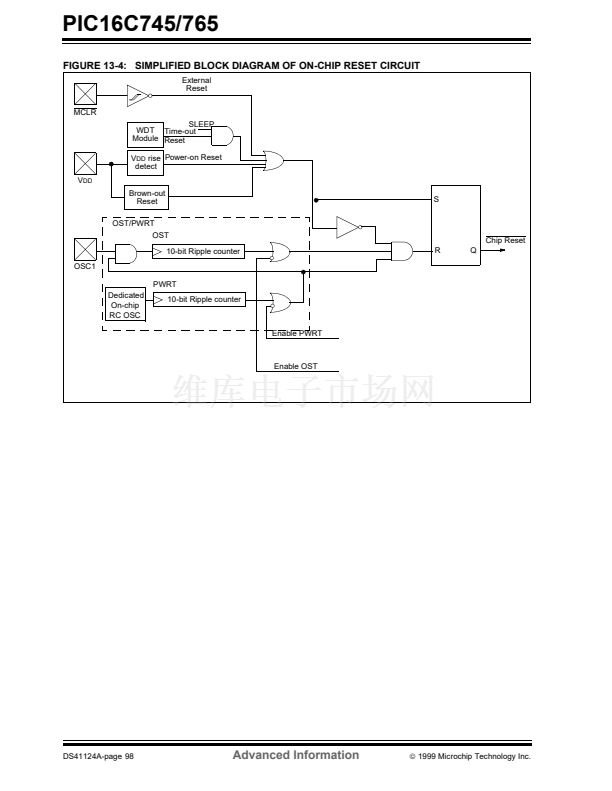
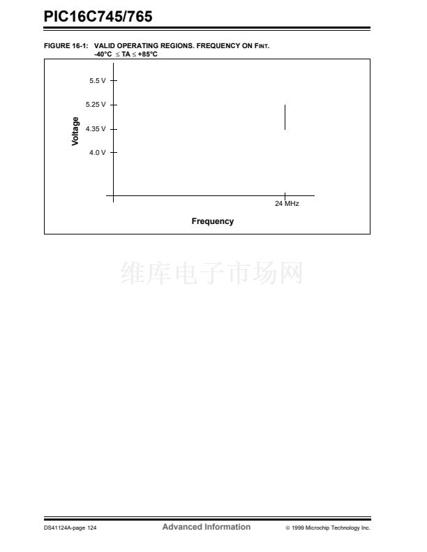
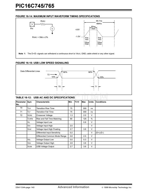
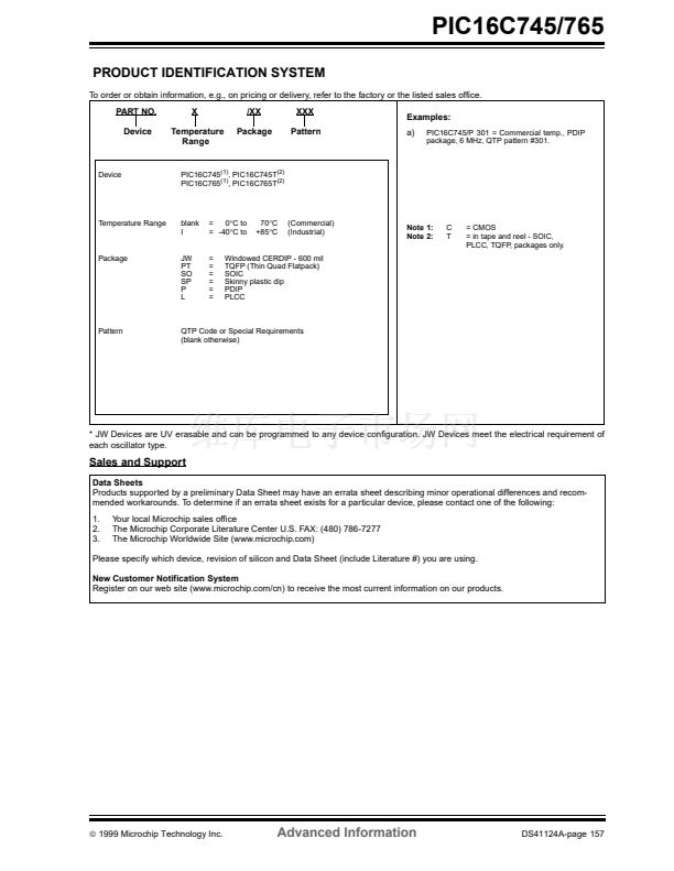
鈥?/div>
2T
OSC
8T
OSC
32T
OSC
Dedicated Internal RC oscillator
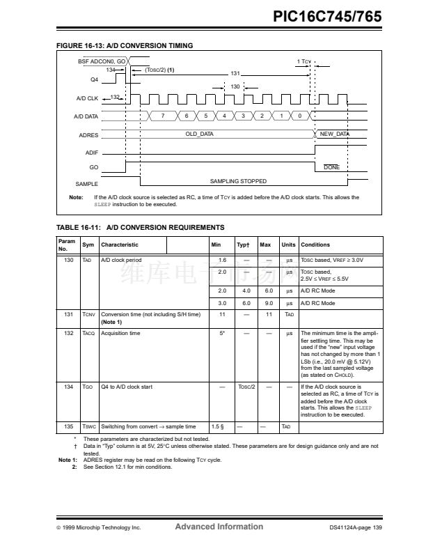
For correct A/D conversions, the A/D conversion clock
(T
AD
) must be selected to ensure a minimum T
AD
time
of 1.6
碌s.
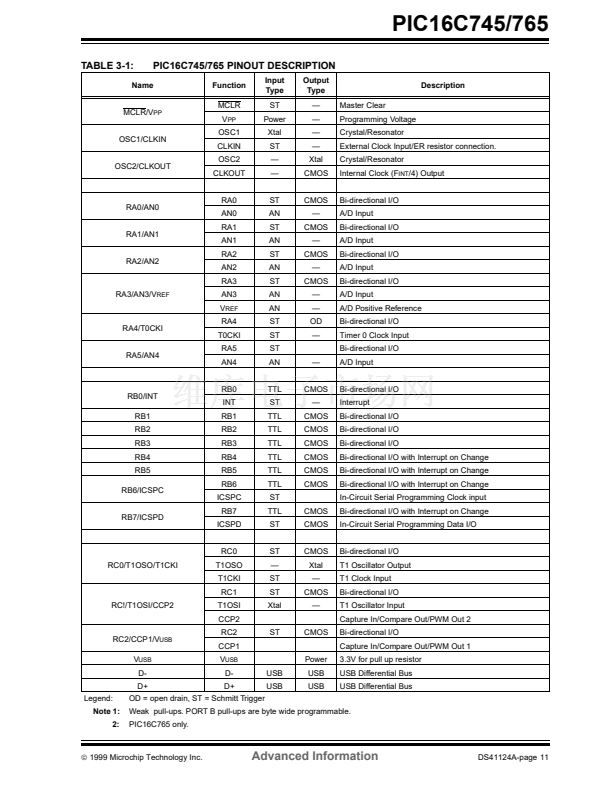
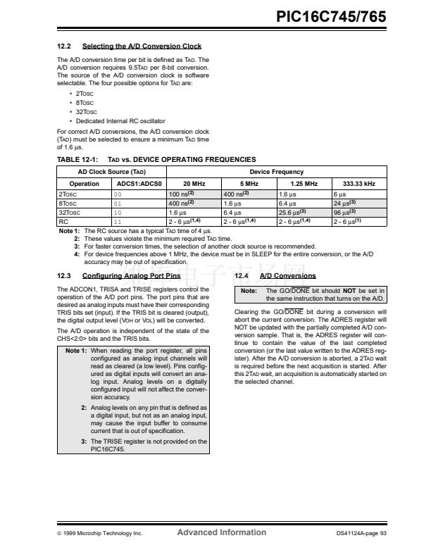
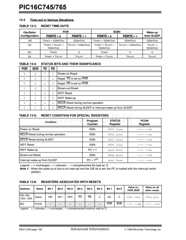
TABLE 12-1:
T
AD
vs. DEVICE OPERATING FREQUENCIES
Device Frequency
20 MHz
5 MHz
1.25 MHz
333.33 kHz
AD Clock Source (T
AD
)
Operation
2T
OSC
8T
OSC
32T
OSC
RC
Note 1:
2:
3:
4:
ADCS1:ADCS0
00
100 ns
(2)
400 ns
(2)
1.6
碌s
6
碌s
01
400 ns
(2)
1.6
碌s
6.4
碌s
24
碌s
(3)
10
1.6
碌s
6.4
碌s
25.6
碌s
(3)
96
碌s
(3)
11
2 - 6
碌s
(1,4)
2 - 6
碌s
(1,4)
2 - 6
碌s
(1,4)
2 - 6
碌s
(1)
The RC source has a typical T
AD
time of 4
碌s.
These values violate the minimum required T
AD
time.
For faster conversion times, the selection of another clock source is recommended.
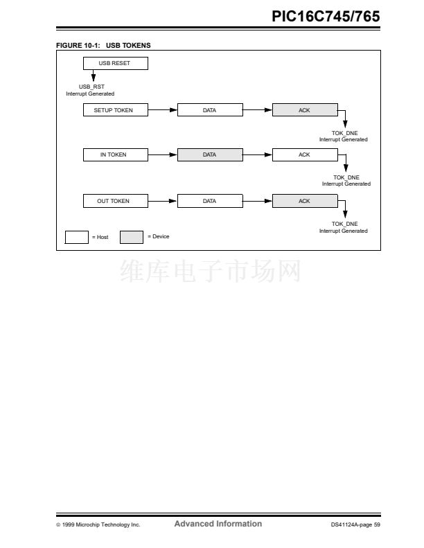
For device frequencies above 1 MHz, the device must be in SLEEP for the entire conversion, or the A/D
accuracy may be out of specification.
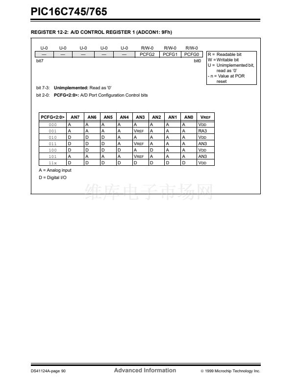
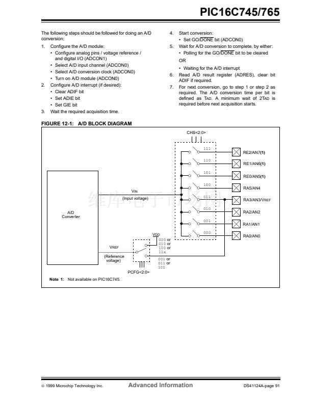
12.3
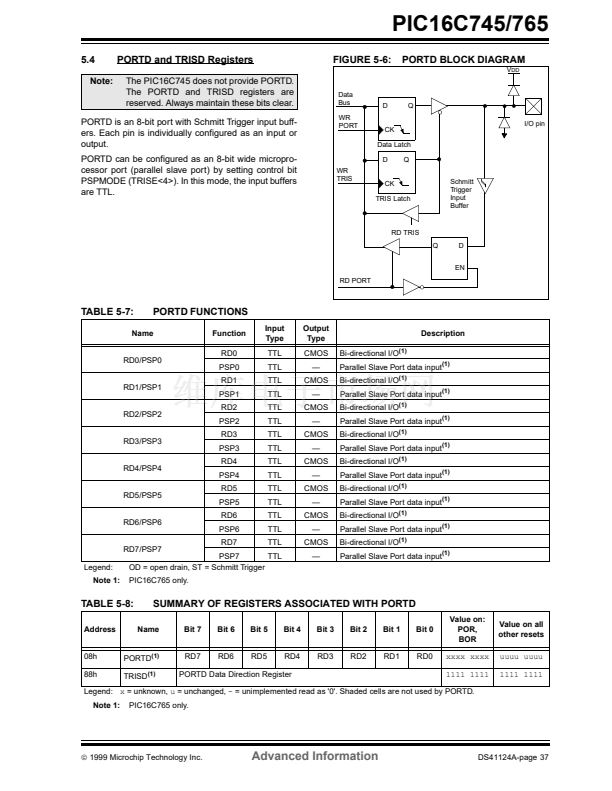
Configuring Analog Port Pins
12.4
Note:
A/D Conversions
The GO/DONE bit should
NOT
be set in
the same instruction that turns on the A/D.
The ADCON1, TRISA and TRISE registers control the
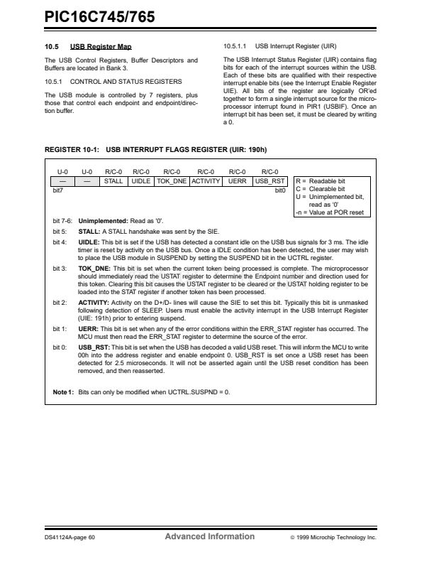
operation of the A/D port pins. The port pins that are
desired as analog inputs must have their corresponding
TRIS bits set (input). If the TRIS bit is cleared (output),
the digital output level (V
OH
or V
OL
) will be converted.
The A/D operation is independent of the state of the
CHS<2:0> bits and the TRIS bits.
Note 1:
When reading the port register, all pins
configured as analog input channels will
read as cleared (a low level). Pins config-
ured as digital inputs will convert an ana-
log input. Analog levels on a digitally
configured input will not affect the conver-
sion accuracy.
2:
Analog levels on any pin that is defined as
a digital input, but not as an analog input,
may cause the input buffer to consume
current that is out of specification.
3:
The TRISE register is not provided on the
PIC16C745.
Clearing the GO/DONE bit during a conversion will
abort the current conversion. The ADRES register will
NOT be updated with the partially completed A/D con-
version sample. That is, the ADRES register will con-
tinue to contain the value of the last completed
conversion (or the last value written to the ADRES reg-
ister). After the A/D conversion is aborted, a 2T
AD
wait
is required before the next acquisition is started. After
this 2T
AD
wait, an acquisition is automatically started on
the selected channel.
漏
1999 Microchip Technology Inc.
Advanced Information
DS41124A-page 93


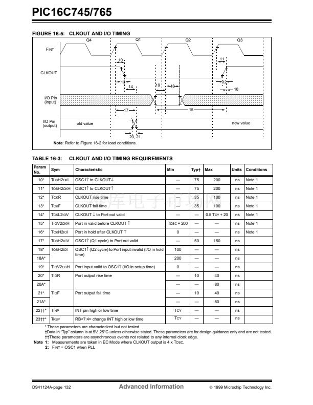
 1
1
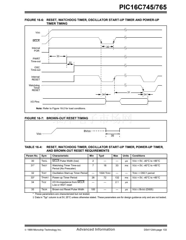
 2
2
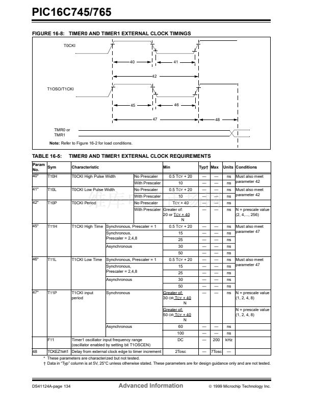
 3
3
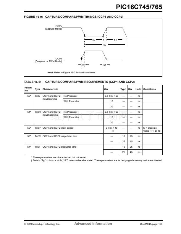
 4
4
 5
5
 6
6
 7
7
 8
8
 9
9
 10
10
 11
11
 12
12
 13
13
 14
14
 15
15
 16
16
 17
17
 18
18
 19
19
 20
20
 21
21
 22
22
 23
23
 24
24
 25
25
 26
26
 27
27
 28
28
 29
29
 30
30
 31
31
 32
32
 33
33
 34
34
 35
35
 36
36
 37
37
 38
38
 39
39
 40
40
 41
41
 42
42
 43
43
 44
44
 45
45
 46
46
 47
47
 48
48
 49
49
 50
50
 51
51
 52
52
 53
53
 54
54
 55
55
 56
56
 57
57
 58
58
 59
59
 60
60
 61
61
 62
62
 63
63
 64
64
 65
65
 66
66
 67
67
 68
68
 69
69
 70
70
 71
71
 72
72
 73
73
 74
74
 75
75
 76
76
 77
77
 78
78
 79
79
 80
80
 81
81
 82
82
 83
83
 84
84
 85
85
 86
86
 87
87
 88
88
 89
89
 90
90
 91
91
 92
92
 93
93
 94
94
 95
95
 96
96
 97
97
 98
98
 99
99
 100
100
 101
101
 102
102
 103
103
 104
104
 105
105
 106
106
 107
107
 108
108
 109
109
 110
110
 111
111
 112
112
 113
113
 114
114
 115
115
 116
116
 117
117
 118
118
 119
119
 120
120
 121
121
 122
122
 123
123
 124
124
 125
125
 126
126
 127
127
 128
128
 129
129
 130
130
 131
131
 132
132
 133
133
 134
134
 135
135
 136
136
 137
137
 138
138
 139
139
 140
140
 141
141
 142
142
 143
143
 144
144
 145
145
 146
146
 147
147
 148
148
 149
149
 150
150
 151
151
 152
152
 153
153
 154
154
 155
155
 156
156
 157
157
 158
158
