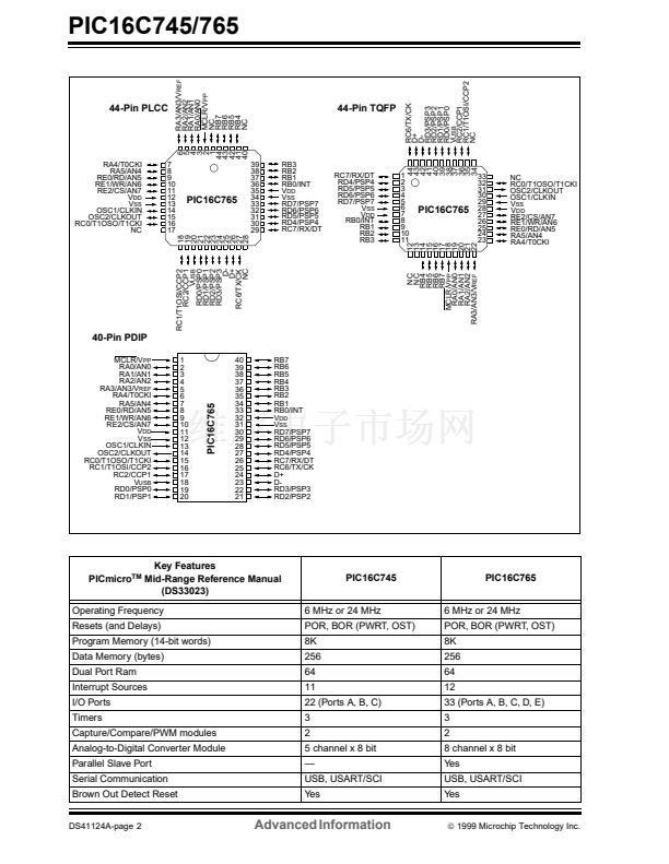
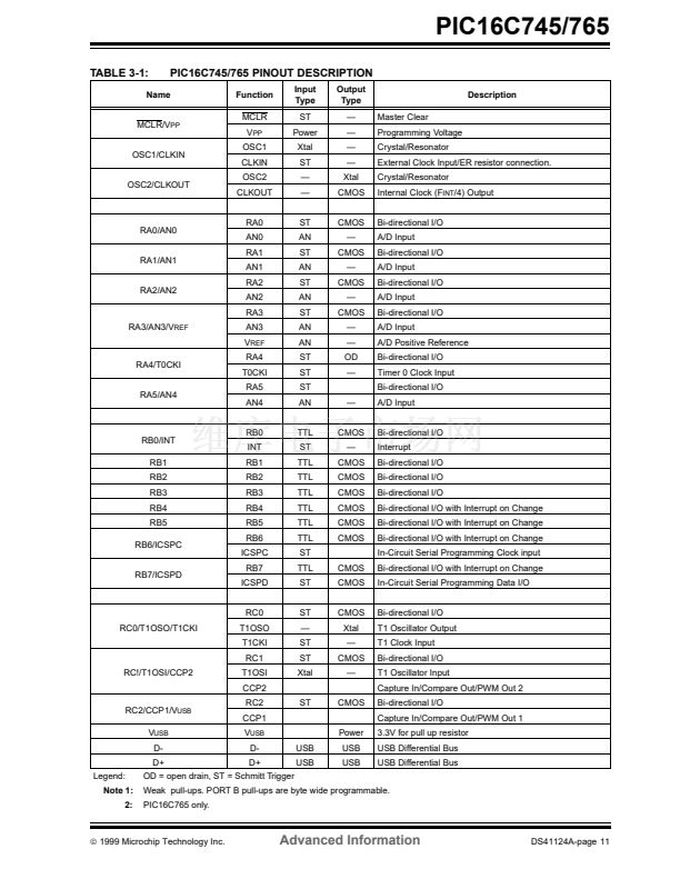
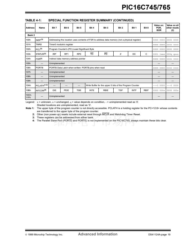
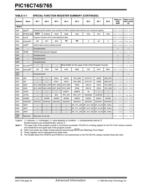
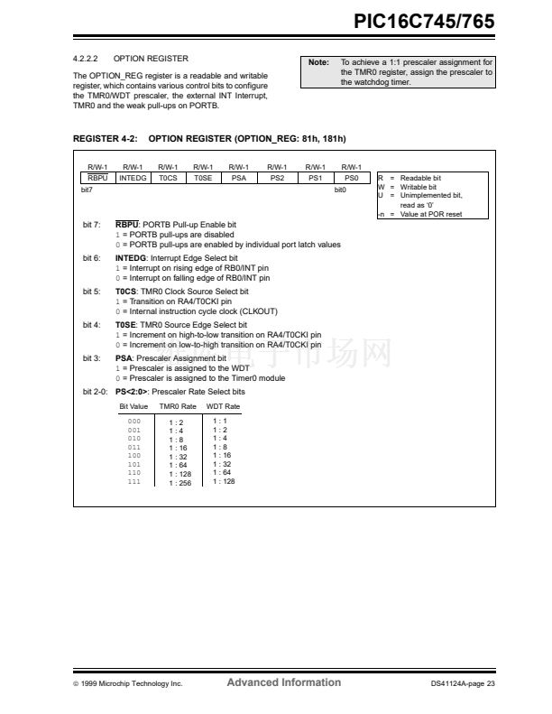
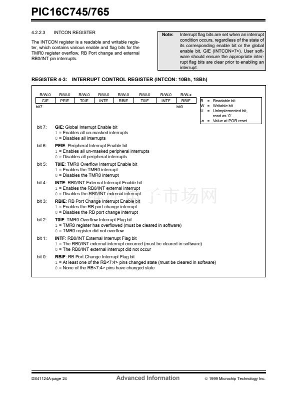
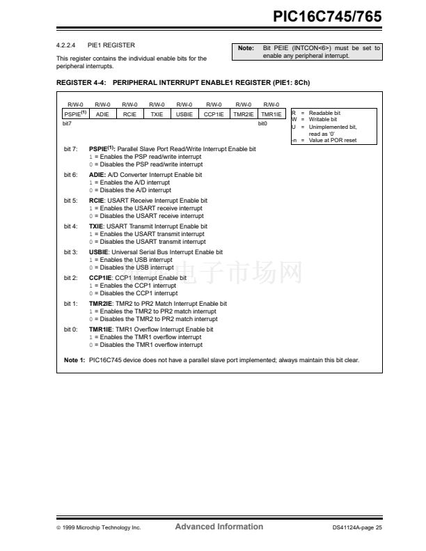
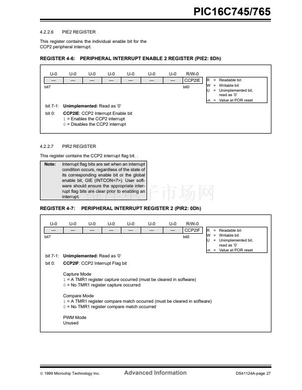
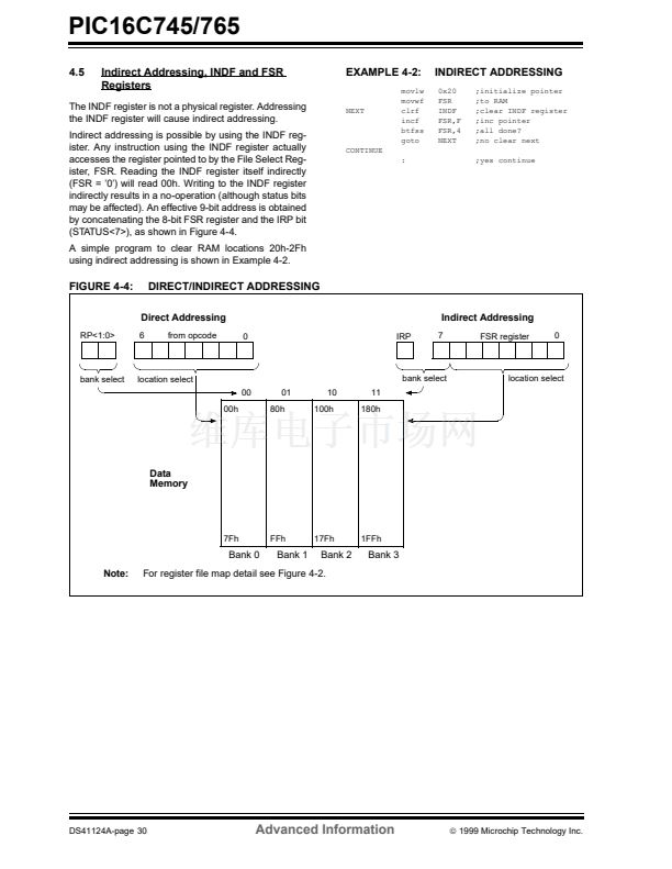
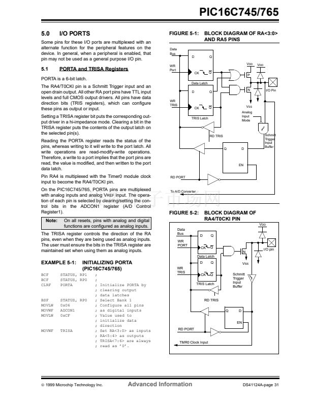
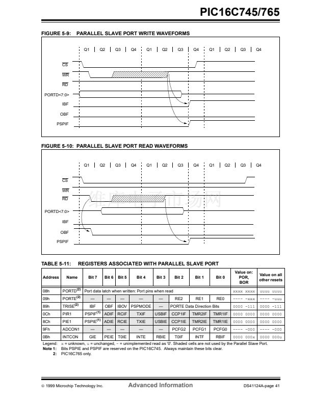
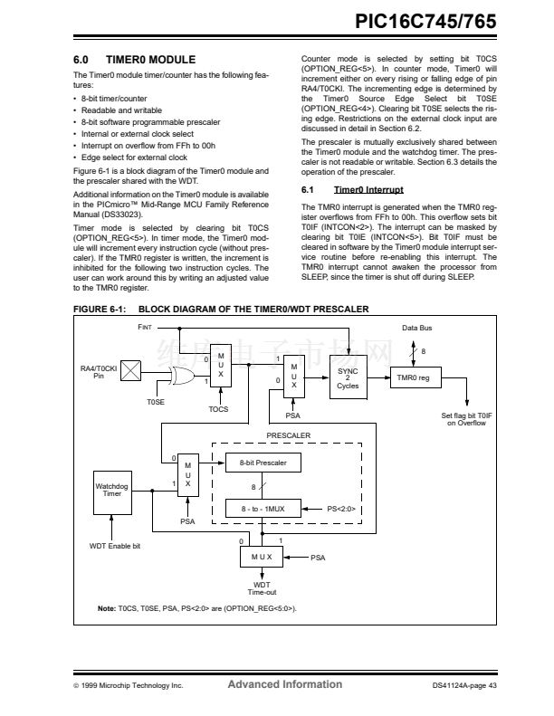
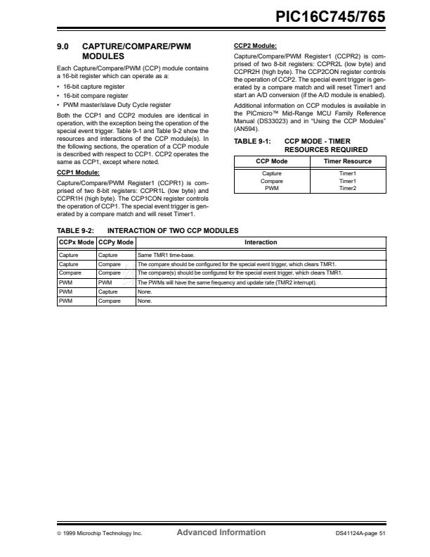
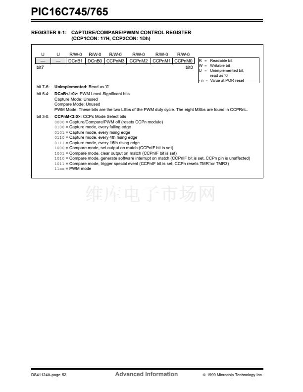
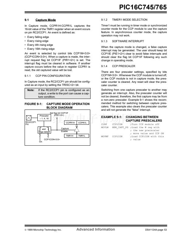
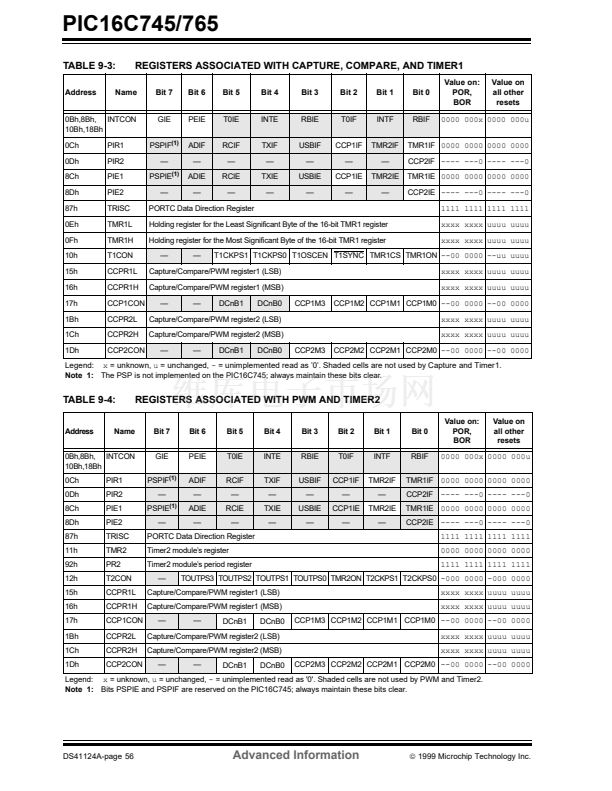
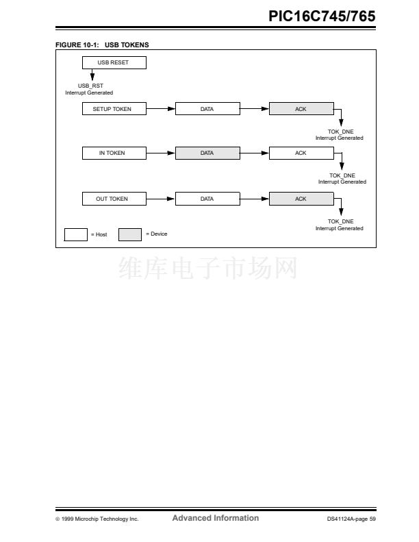
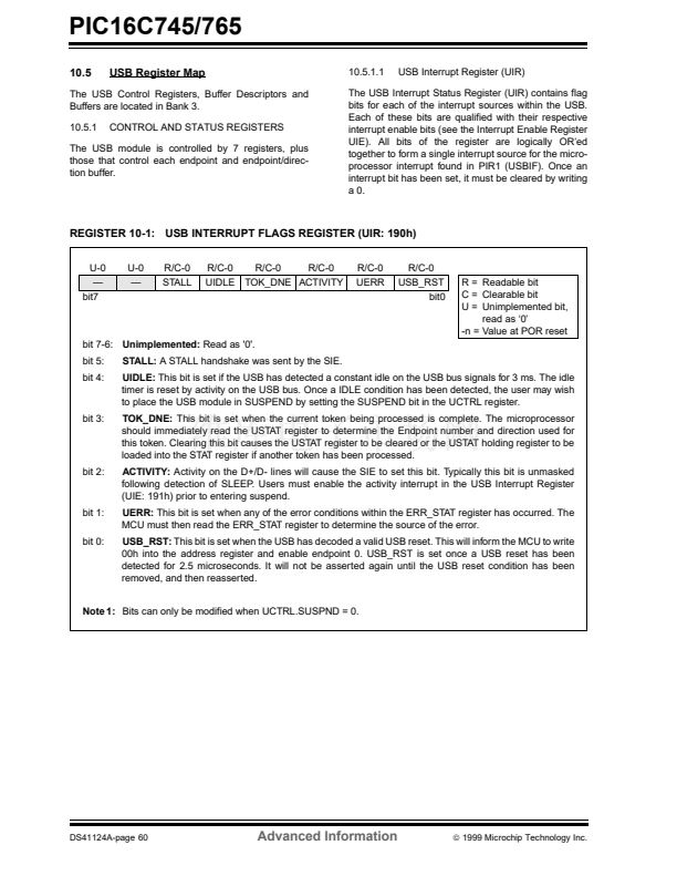
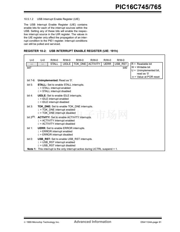
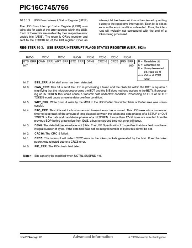
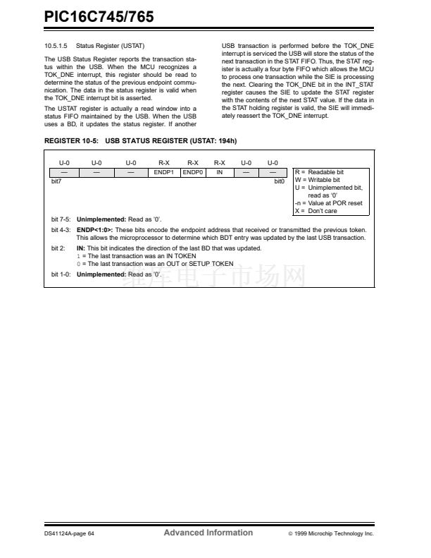
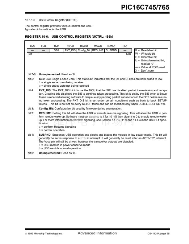
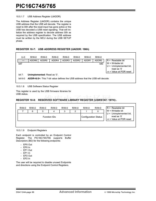
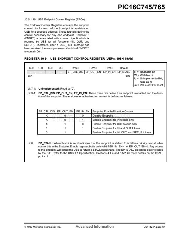
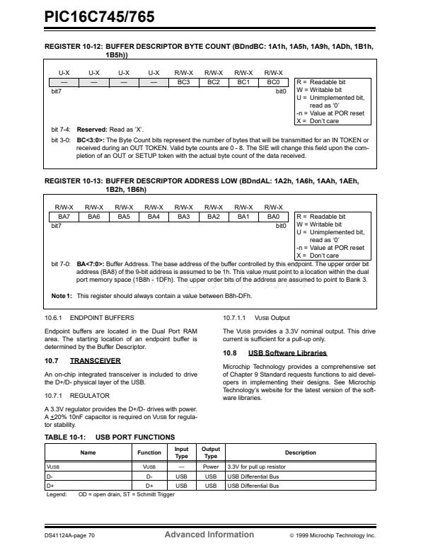
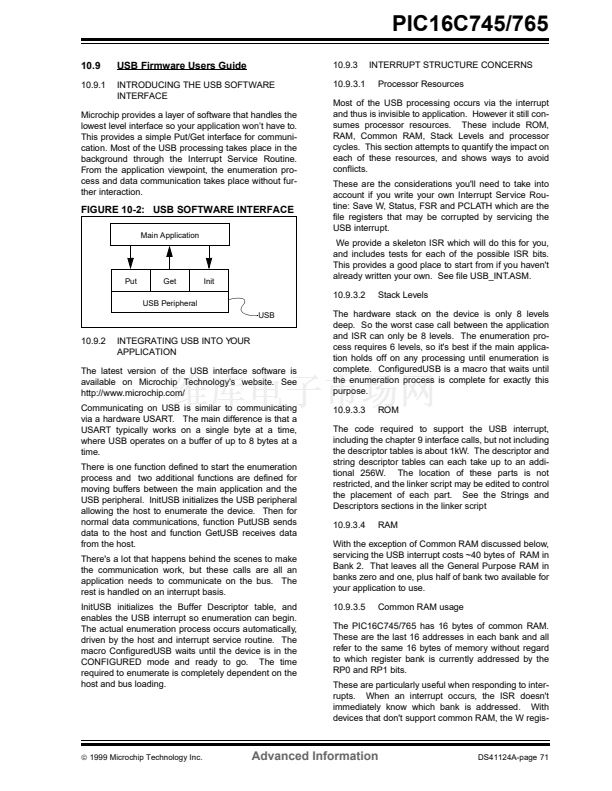
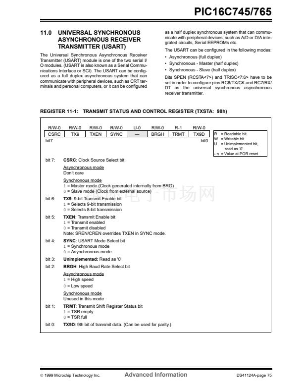
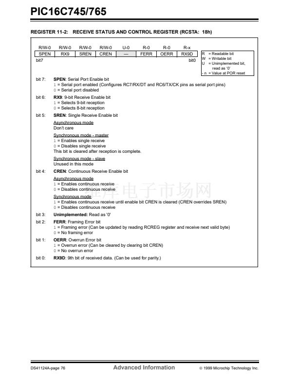
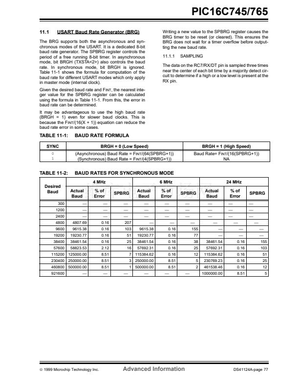
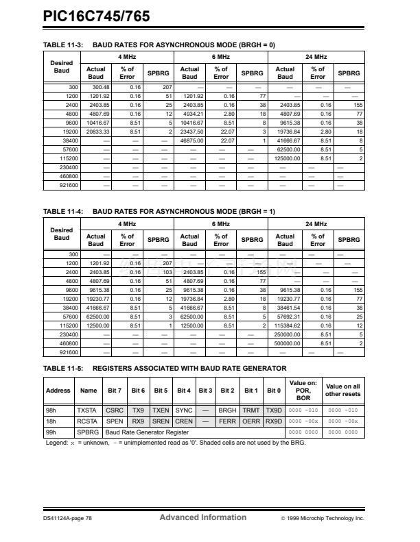
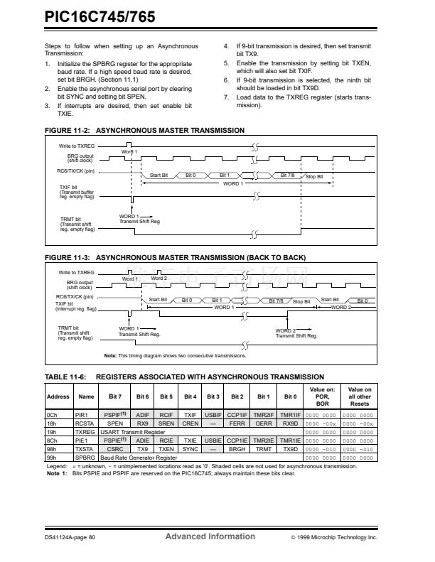
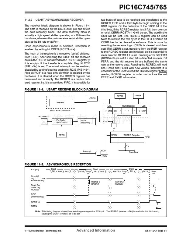
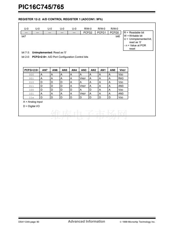
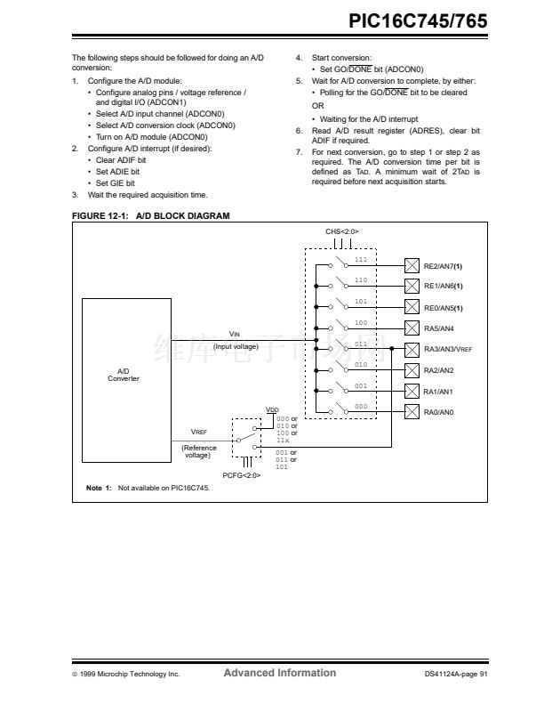
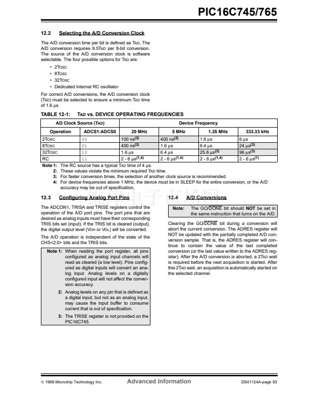
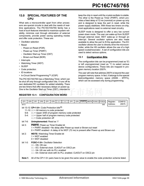
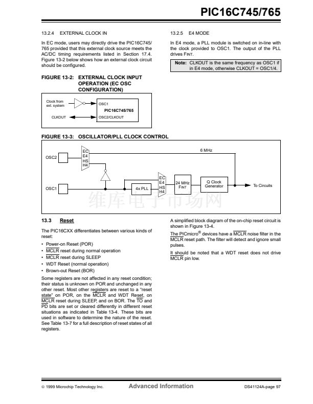
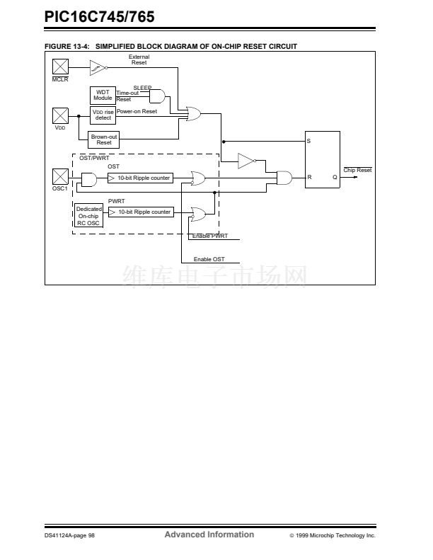
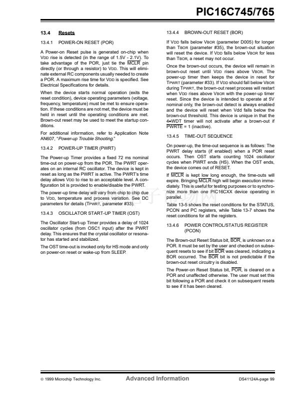
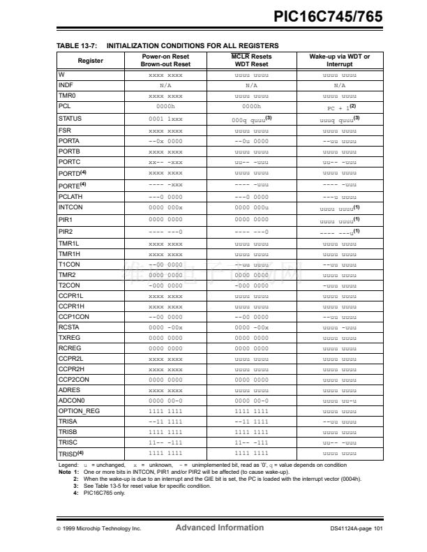
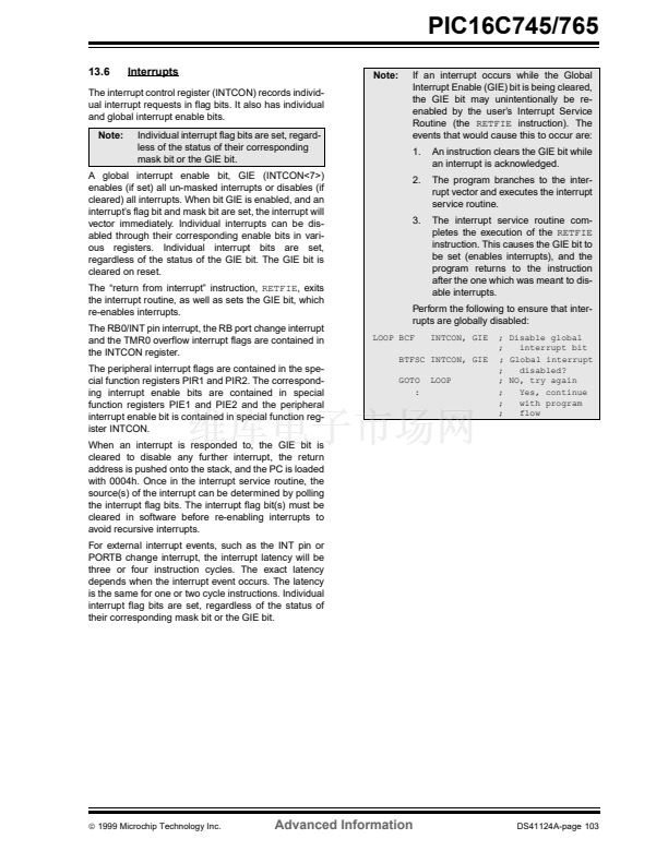
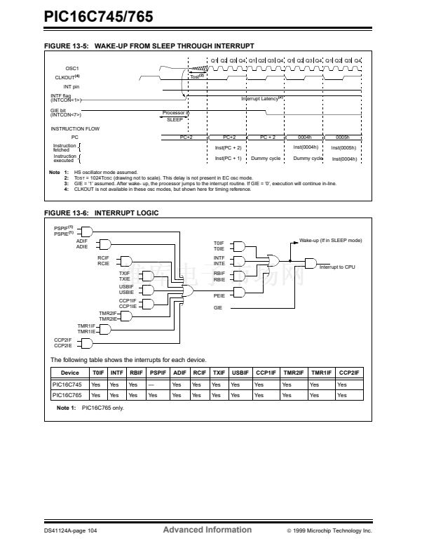
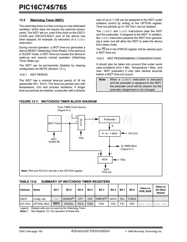
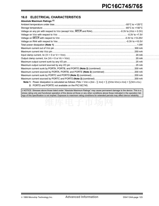
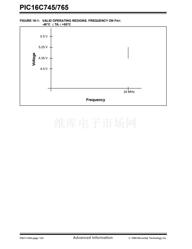
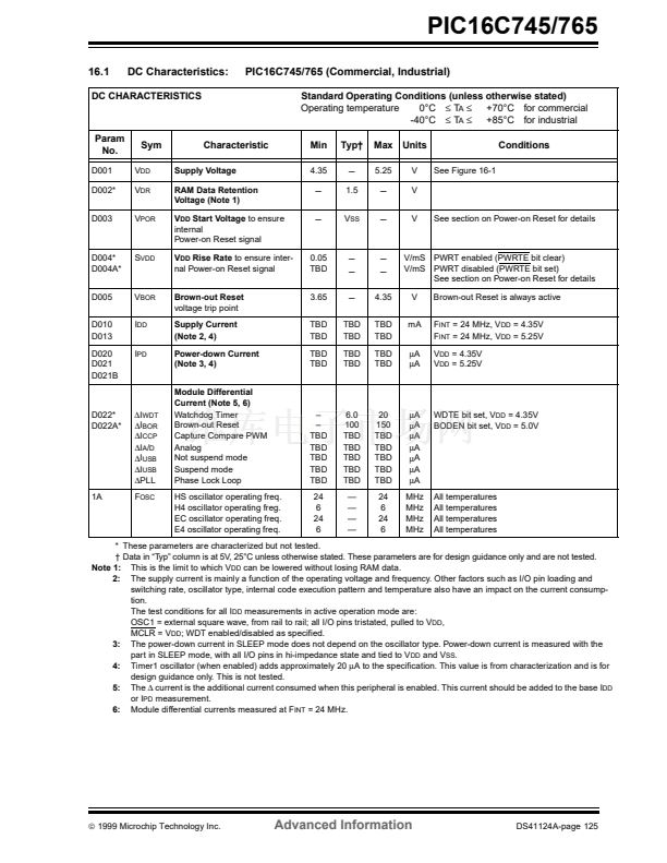
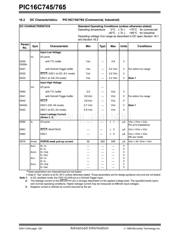
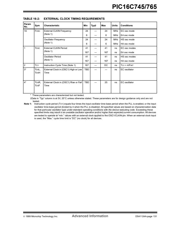
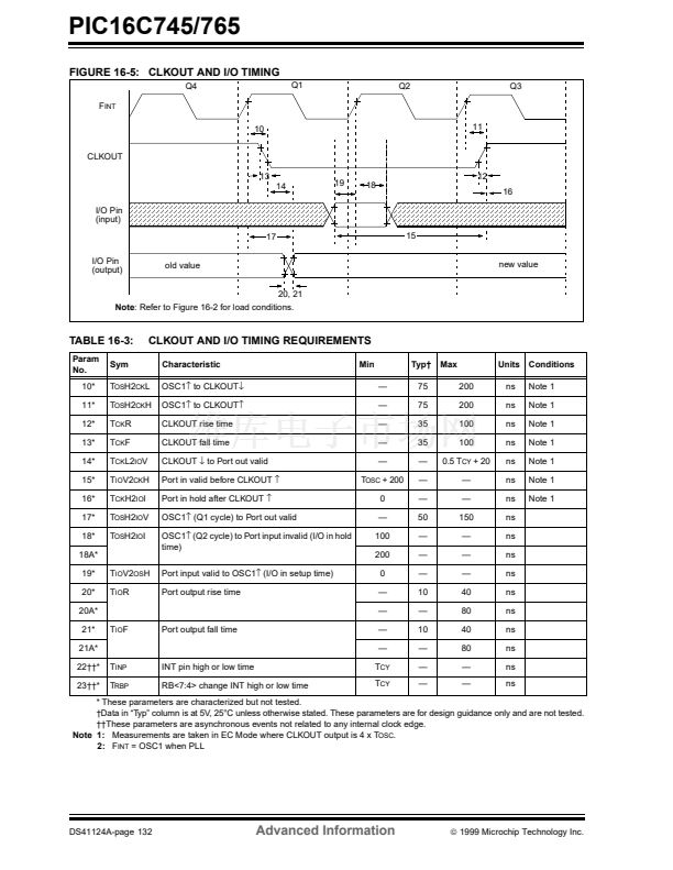
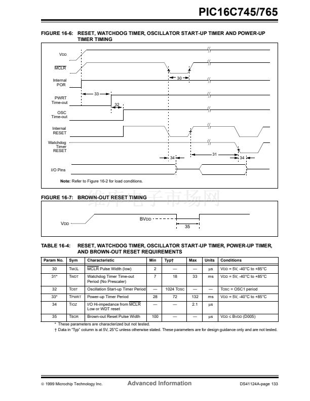
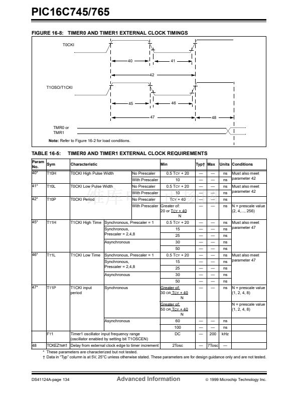
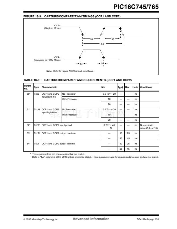
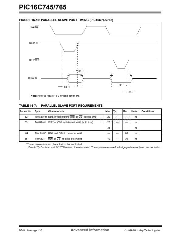
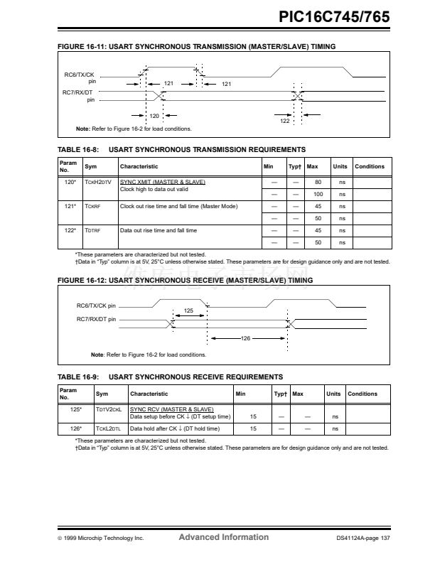
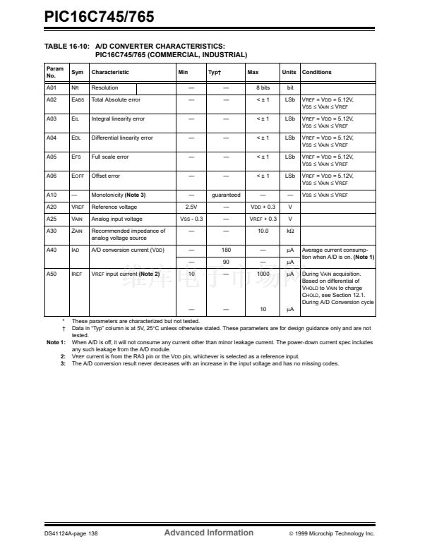
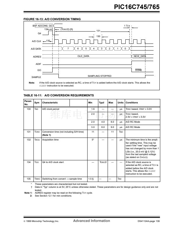
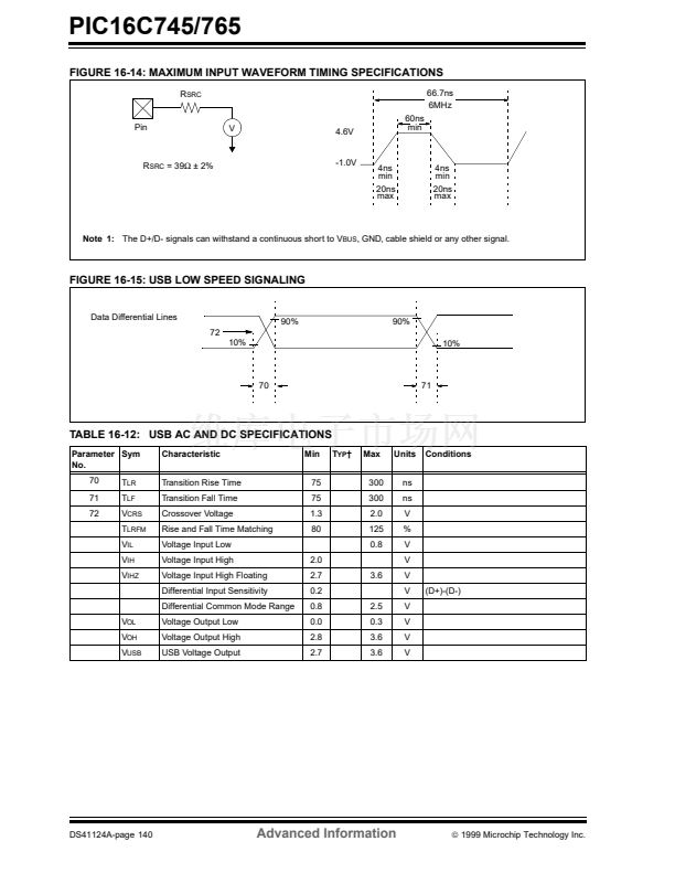
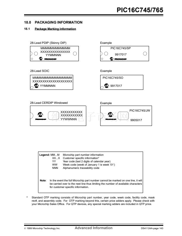
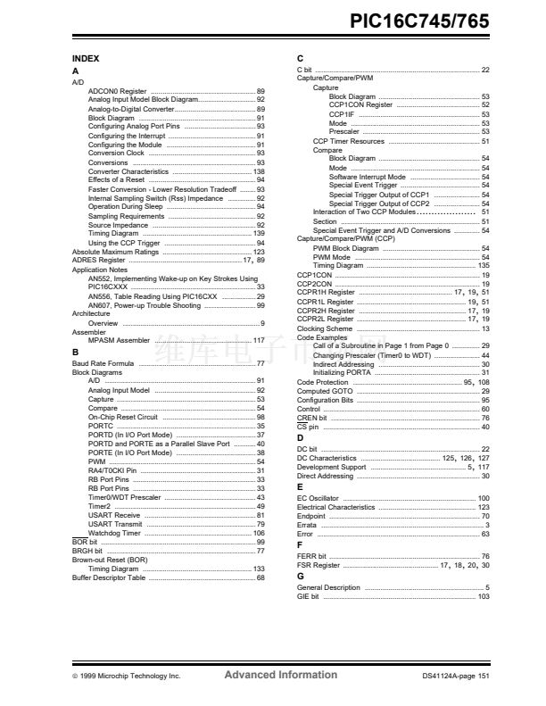
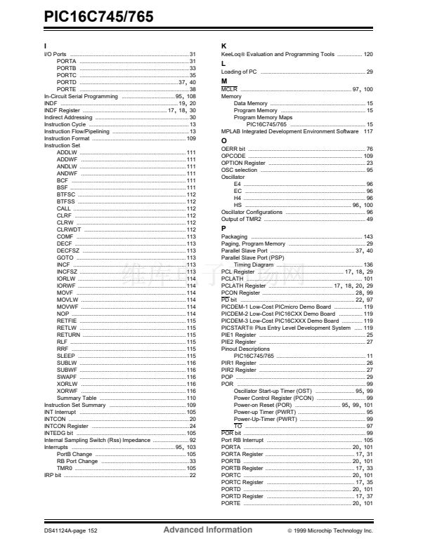
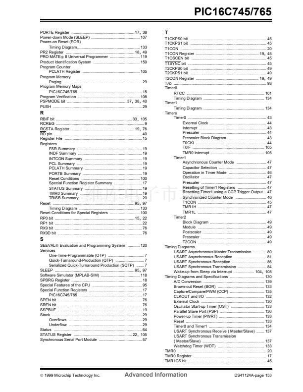
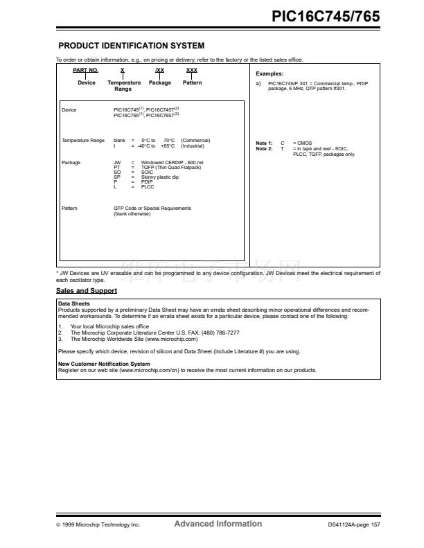
PIC16C745/765
11.2.2
USART ASYNCHRONOUS RECEIVER
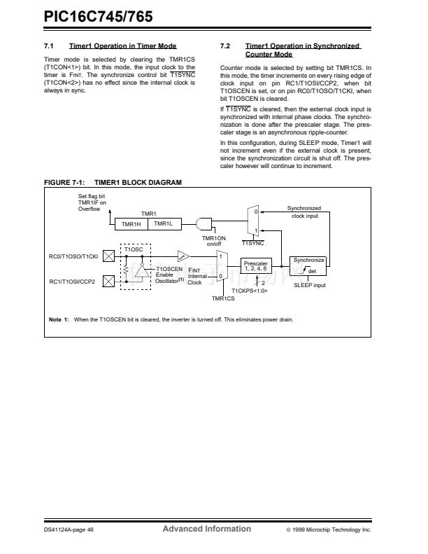
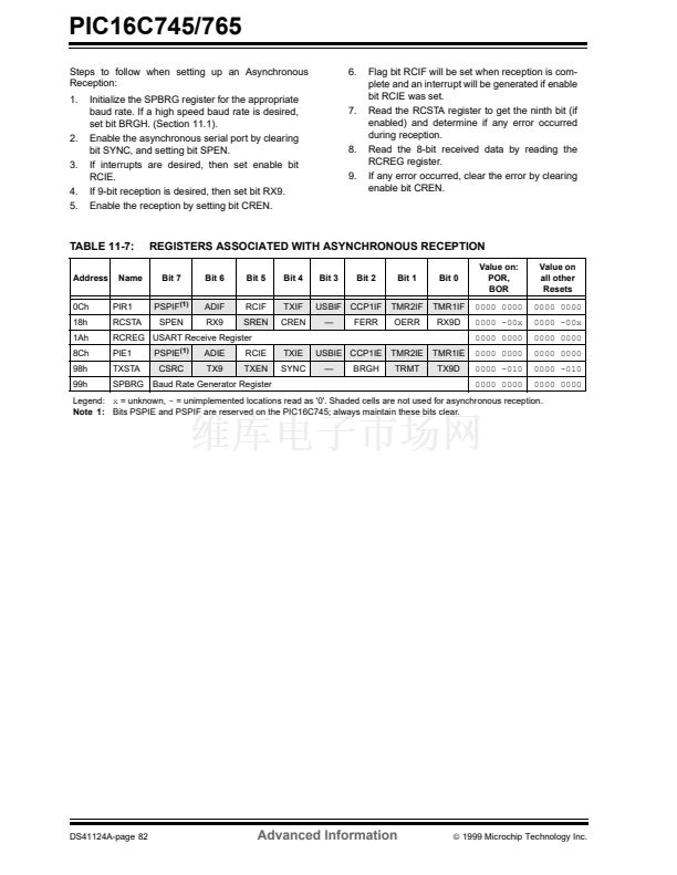
The receiver block diagram is shown in Figure 11-4.
The data is received on the RC7/RX/DT pin and drives
the data recovery block. The data recovery block is
actually a high speed shifter operating at x16 times the
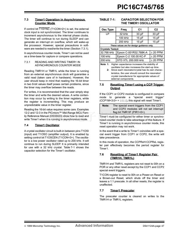
baud rate, whereas the main receive serial shifter oper-
ates at the bit rate or at F
INT
.
Once asynchronous mode is selected, reception is
enabled by setting bit CREN (RCSTA<4>).
The heart of the receiver is the receive (serial) shift reg-
ister (RSR). After sampling the STOP bit, the received
data in the RSR is transferred to the RCREG register (if
it is empty). If the transfer is complete, flag bit RCIF
(PIR1<5>) is set. The actual interrupt can be enabled/
disabled by setting/clearing enable bit RCIE (PIE1<5>).
Flag bit RCIF is a read only bit which is cleared by the
hardware. It is cleared when the RCREG register has
been read and is empty. The RCREG is a double buff-
ered register, i.e. it is a two deep FIFO. It is possible for
two bytes of data to be received and transferred to the
RCREG FIFO and a third byte to begin shifting to the
RSR register. On the detection of the STOP bit of the
third byte, if the RCREG register is still full, then overrun
error bit OERR (RCSTA<1>) will be set. The word in the
RSR will be lost. The RCREG register can be read
twice to retrieve the two bytes in the FIFO. Overrun bit
OERR has to be cleared in software. This is done by
resetting the receive logic (CREN is cleared and then
set). If bit OERR is set, transfers from the RSR register
to the RCREG register are inhibited, so it is essential to
clear error bit OERR if it is set. Framing error bit FERR
(RCSTA<2>) is set if a stop bit is detected as clear. Bit
FERR and the 9th receive bit are buffered the same
way as the receive data. Reading the RCREG, will load
bits RX9D and FERR with new values, therefore it is
essential for the user to read the RCSTA register before
reading RCREG register in order not to lose the old
FERR and RX9D information.
FIGURE 11-4: USART RECEIVE BLOCK DIAGRAM
OERR
CREN
SPBRG
MSb
Baud Rate Generator
RC7/RX/DT
Pin Buffer
and Control
Data
Recovery
RX9
Stop (8)
7
RSR Register
鈥?鈥?鈥?/div>
1
LSb
0 Start
FERR
SPEN
RX9D
RCREG Register
FIFO
8
Interrupt
RCIF
RCIE
Data Bus
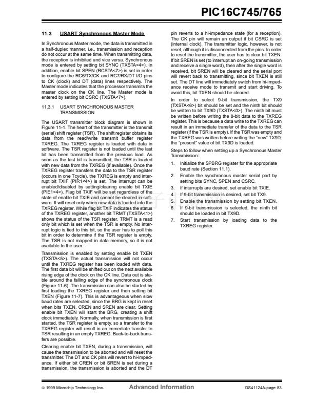
FIGURE 11-5: ASYNCHRONOUS RECEPTION
RX (pin)
Rcv shift
reg
Rcv buffer reg
Read Rcv
buffer reg
RCREG
RCIF
(interrupt flag)
OERR bit
CREN
Note:
This timing diagram shows three words appearing on the RX input. The RCREG (receive buffer) is read after the third word,
causing the OERR (overrun) bit to be set.
Start
bit
bit0
bit1
bit7/8 Stop
bit
Start
bit
bit0
bit7/8
Stop
bit
Start
bit
bit7/8
Stop
bit
WORD 1
RCREG
WORD 2
RCREG
漏
1999 Microchip Technology Inc.
Advanced Information
DS41124A-page 81


 1
1
 2
2
 3
3
 4
4
 5
5
 6
6
 7
7
 8
8
 9
9
 10
10
 11
11
 12
12
 13
13
 14
14
 15
15
 16
16
 17
17
 18
18
 19
19
 20
20
 21
21
 22
22
 23
23
 24
24
 25
25
 26
26
 27
27
 28
28
 29
29
 30
30
 31
31
 32
32
 33
33
 34
34
 35
35
 36
36
 37
37
 38
38
 39
39
 40
40
 41
41
 42
42
 43
43
 44
44
 45
45
 46
46
 47
47
 48
48
 49
49
 50
50
 51
51
 52
52
 53
53
 54
54
 55
55
 56
56
 57
57
 58
58
 59
59
 60
60
 61
61
 62
62
 63
63
 64
64
 65
65
 66
66
 67
67
 68
68
 69
69
 70
70
 71
71
 72
72
 73
73
 74
74
 75
75
 76
76
 77
77
 78
78
 79
79
 80
80
 81
81
 82
82
 83
83
 84
84
 85
85
 86
86
 87
87
 88
88
 89
89
 90
90
 91
91
 92
92
 93
93
 94
94
 95
95
 96
96
 97
97
 98
98
 99
99
 100
100
 101
101
 102
102
 103
103
 104
104
 105
105
 106
106
 107
107
 108
108
 109
109
 110
110
 111
111
 112
112
 113
113
 114
114
 115
115
 116
116
 117
117
 118
118
 119
119
 120
120
 121
121
 122
122
 123
123
 124
124
 125
125
 126
126
 127
127
 128
128
 129
129
 130
130
 131
131
 132
132
 133
133
 134
134
 135
135
 136
136
 137
137
 138
138
 139
139
 140
140
 141
141
 142
142
 143
143
 144
144
 145
145
 146
146
 147
147
 148
148
 149
149
 150
150
 151
151
 152
152
 153
153
 154
154
 155
155
 156
156
 157
157
 158
158
