鈥?/div>
40掳C to +85掳C
Pin and function compatible to the MPC972
MPC9772
3.3V 1:12 LVCMOS
PLL CLOCK GENERATOR
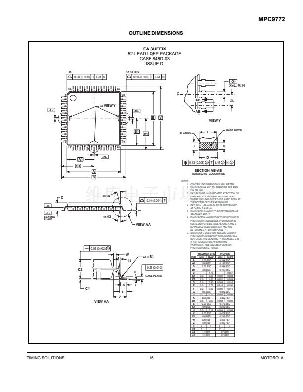
FA SUFFIX
52 LEAD LQFP PACKAGE
CASE 848D
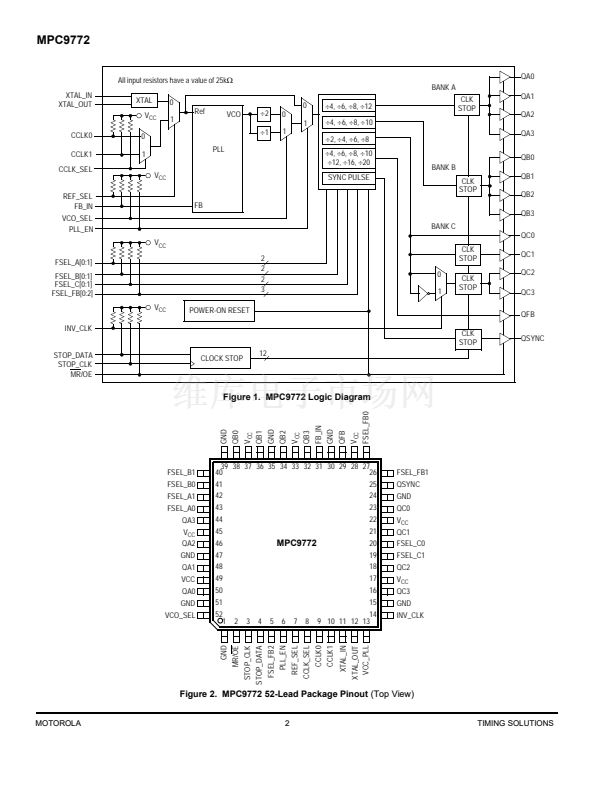
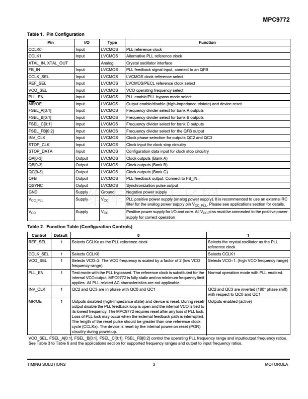
Functional Description
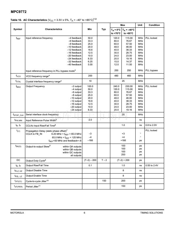
The MPC9772 utilizes PLL technology to frequency lock its outputs onto an input reference clock. Normal operation of the
MPC9772 requires the connection of the PLL feedback output QFB to feedback input FB_IN to close the PLL feedback path. The
reference clock frequency and the divider for the feedback path determine the VCO frequency. Both must be selected to match the
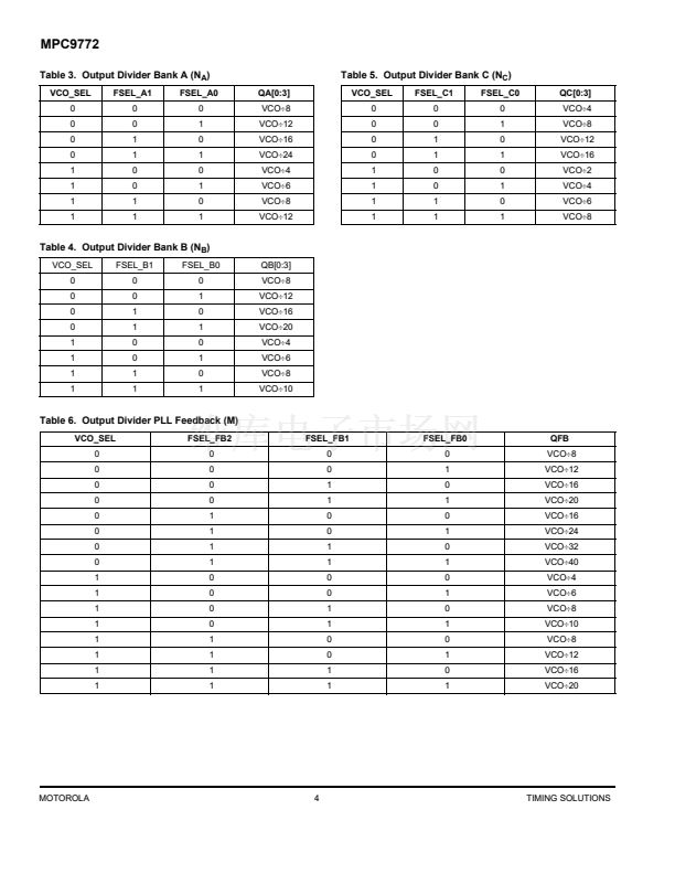
VCO frequency range. The MPC9772 features an extensive level of frequency programmability between the 12 outputs as well as
the output to input relationships, for instance 1:1, 2:1, 3:1, 3:2, 4:1, 4:3, 5:1, 5:2, 5:3, 5:4, 5:6, 6:1, 8:1 and 8:3.
The QSYNC output will indicate when the coincident rising edges of the above relationships will occur. The selectability of the feed-
back frequency is independent of the output frequencies. This allows for very flexible programming of the input reference versus out-
put frequency relationship. The output frequencies can be either odd or even multiples of the input reference. In addition the output
frequency can be less than the input frequency for applications where a frequency needs to be reduced by a non-binary factor. The
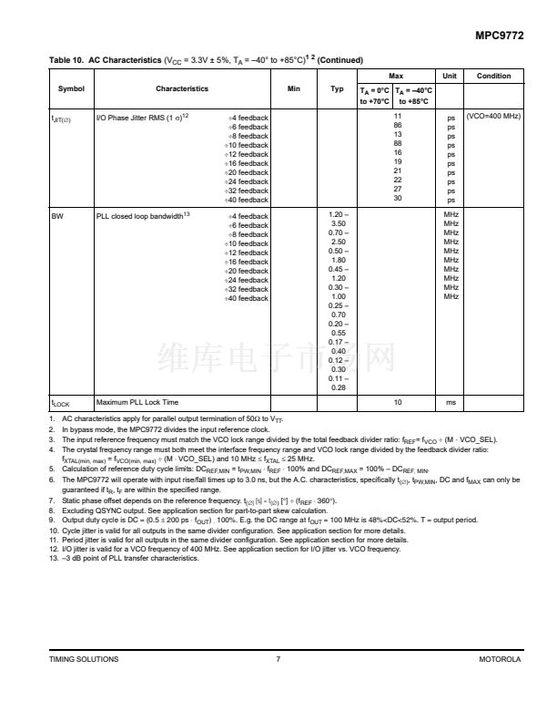
MPC9772 also supports the 180掳 phase shift of one of its output banks with respect to the other output banks. The QSYNC outputs
reflects the phase relationship between the QA and QC outputs and can be used for the generation of system baseline timing signals.
The REF_SEL pin selects the internal crystal oscillator or the LVCMOS compatible inputs as the reference clock signal. Two alter-
native LVCMOS compatible clock inputs are provided for clock redundancy support. The PLL_EN control selects the PLL bypass con-
figuration for test and diagnosis. In this configuration, the selected input reference clock is routed directly to the output dividers
bypassing the PLL. The PLL bypass is fully static and the minimum clock frequency specification and all other PLL characteristics do
not apply.
The outputs can be individually disabled (stopped in logic low state) by programming the serial CLOCK_STOP interface of the
MPC9772. The MPC9772 has an internal power-on reset.
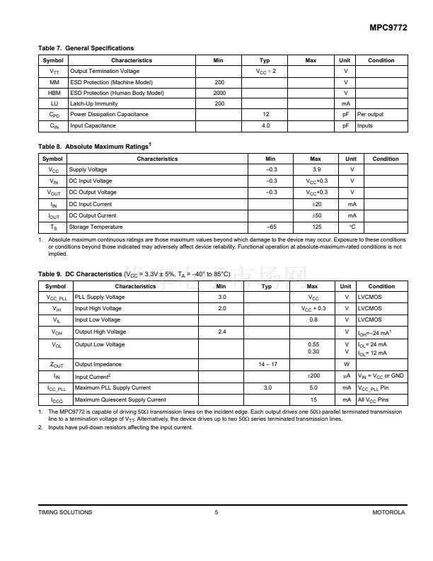
The MPC9772 is fully 3.3V compatible and requires no external loop filter components. All inputs (except XTAL) accept LVCMOS
signals while the outputs provide LVCMOS compatible levels with the capability to drive terminated 50
鈩?/div>
transmission lines. For series
terminated transmission lines, each of the MPC9772 outputs can drive one or two traces giving the devices an effective fanout of 1:24.
The device is pin and function compatible to the MPC972 and is packaged in a 52-lead LQFP package.
漏 Motorola, Inc. 2004


 1
1
 2
2
 3
3
 4
4
 5
5
 6
6
 7
7
 8
8
 9
9
 10
10
 11
11
 12
12
 13
13
 14
14
 15
15
 16
16
