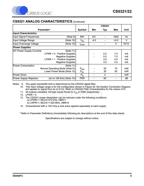
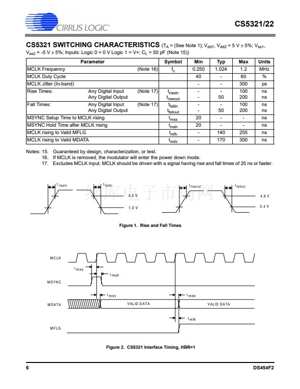
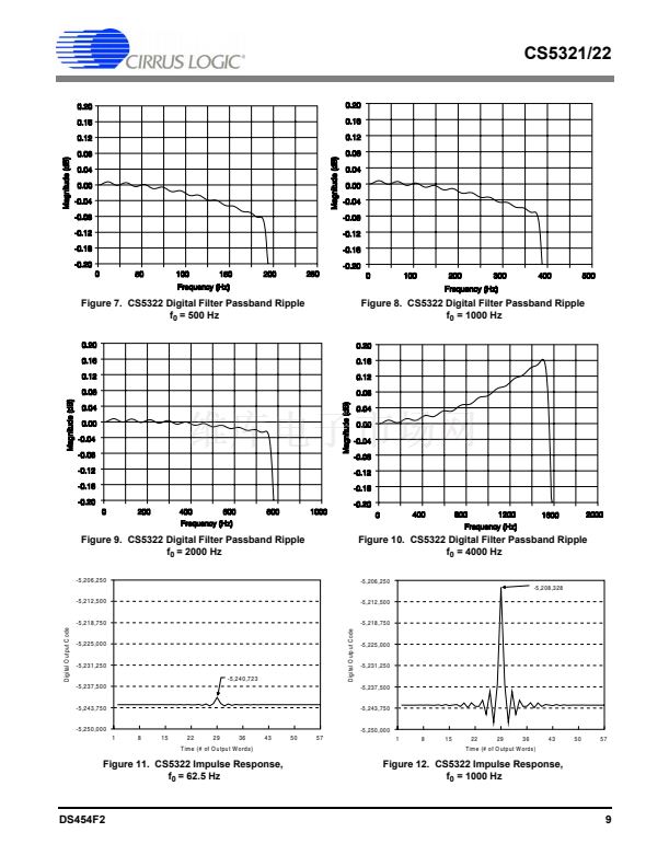
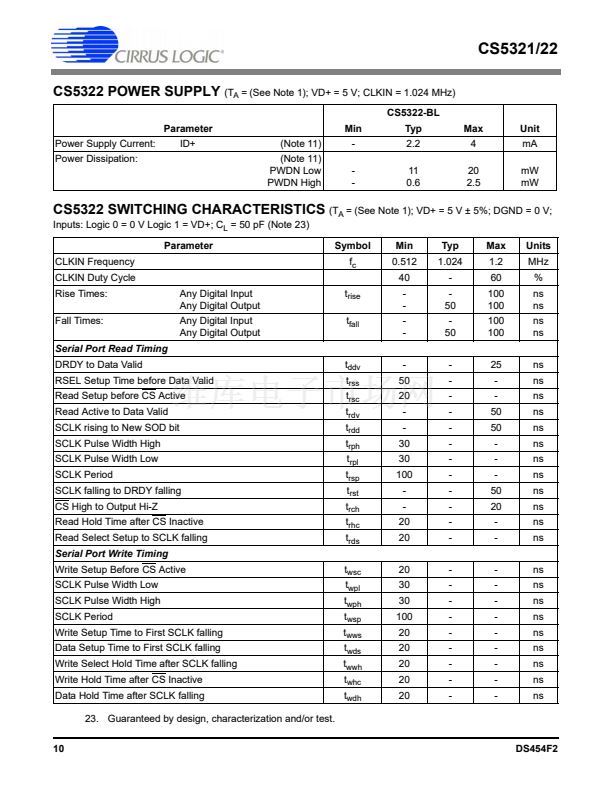
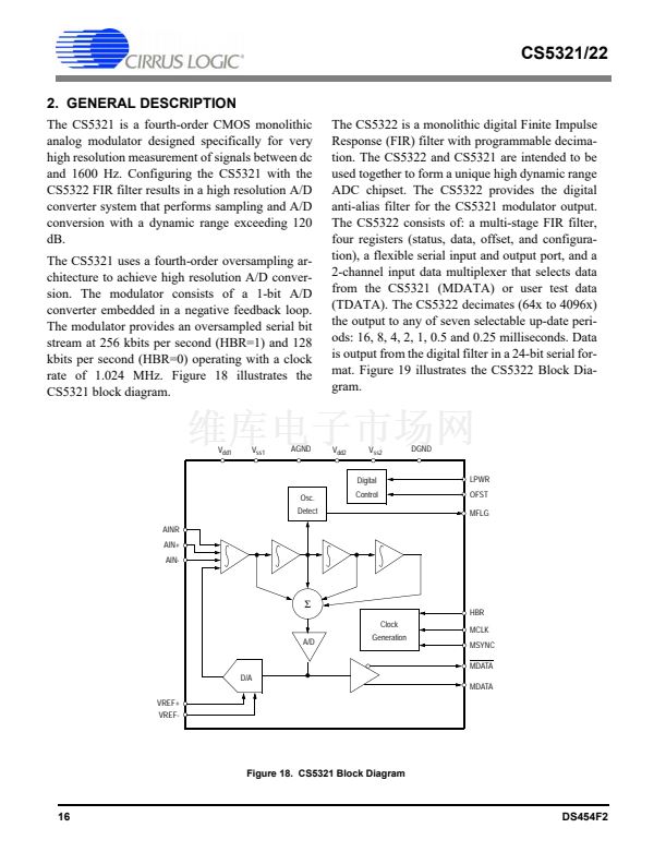
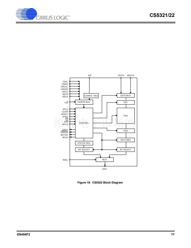
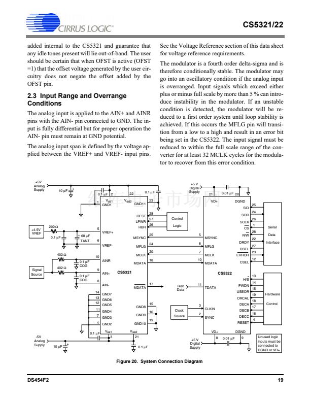
CS5321/22
SOD - Serial Output Data, Pin 24
The output coding is 2鈥檚 complement with the data bits presented MSB first, LSB last. Data
changes on the rising edge of SCLK. An internal nominal 100 k鈩?pull-up resistor is included.
Digital Inputs
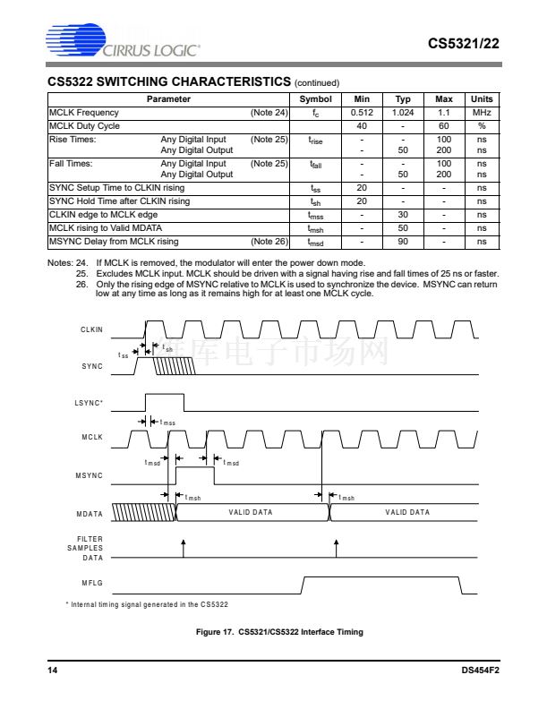
MDATA 鈥?Modulator Data, Pin 10
Data will be presented in a one-bit serial data stream at a bit rate of 256 kHz; (CLKIN =
1.024 MHz).
TDATA - Test Data, Pin 11
Input for user test data.
MFLG 鈥?Modulator Flag, Pin 6
A transition from a low to high level signals that the CS5321 modulator is unstable due to an
over-range on the analog input. A Status Bit will be set in the digital filter indicating an error
condition. An internal nominal 100 k鈩?pull-down resistor included on the input pin.
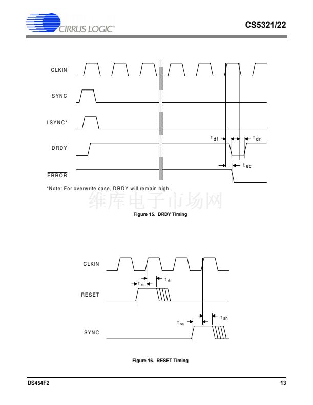
RESET - Filter Reset, Pin 4
Performs a hard reset on the chip, all registers and accumulators are cleared. All signals to the
device are locked out except CLKIN. The error flags in the Status Register are set to zero and
the Data Register and Offset Register are set to zero. The configuration register is set to the
values of the corresponding input pins. SYNC must be applied to resume convolutions after
RESET deasserts.
CLKIN - Clock Input, Pin 3
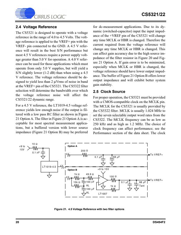
A CMOS-Compatible clock input to this pin (nominally 1.024 MHz) provides the necessary
clock for operation the modulator and filter.
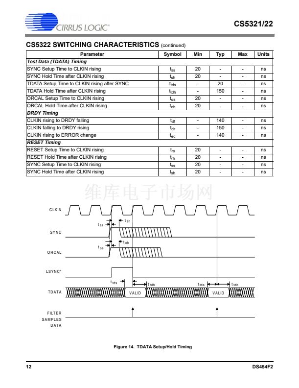
SYNC - Frame Sync, Pin 2
Conversion synchronization input. This signal synchronizes the start of the filter convolution.
More than one SYNC signal can occur with no effect on filter performance, providing the
SYNC signals are perfectly timed at intervals equal to the output sample period.
CSEL - Channel Select, Pin 12
When high, information on the TDATA pin is presented to the digital filter. A low causes data
on the MDATA input to be presented to the digital filter.
PWDN - Powerdown, Pin 14
Powers down the filter when taken high. Convolution cycles in the digital filter and the MCLK
signal are stopped. The registers maintain their data and the serial port remains active. SYNC
must be applied to resume convolutions after PWDN deasserts.
DECA - Decimation Rate Control, Pin 18
See Table 4.
DECB - Decimation Rate Control, Pin 17
See Table 4.
32
DS454F2


 1
1
 2
2
 3
3
 4
4
 5
5
 6
6
 7
7
 8
8
 9
9
 10
10
 11
11
 12
12
 13
13
 14
14
 15
15
 16
16
 17
17
 18
18
 19
19
 20
20
 21
21
 22
22
 23
23
 24
24
 25
25
 26
26
 27
27
 28
28
 29
29
 30
30
 31
31
 32
32
 33
33
 34
34
 35
35
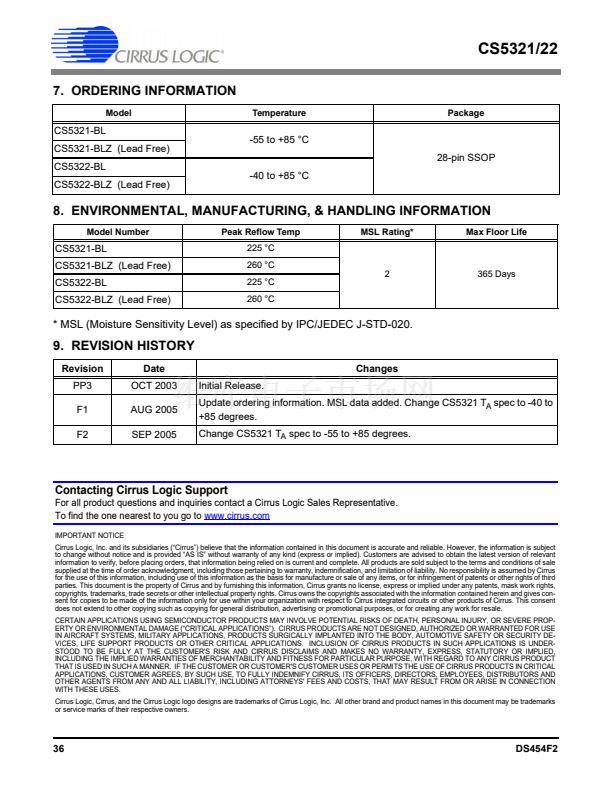 36
36
