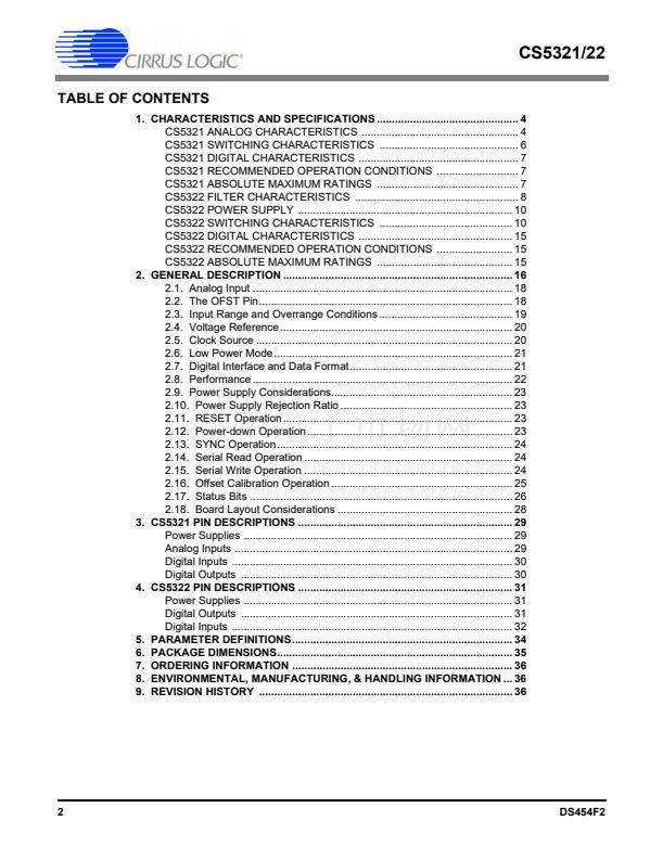
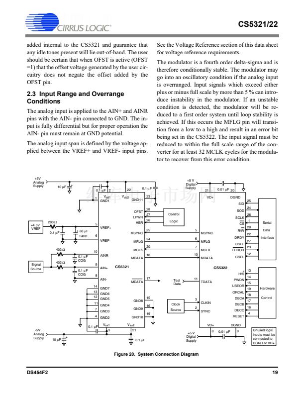
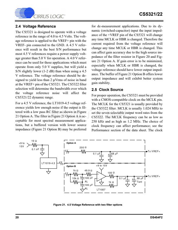
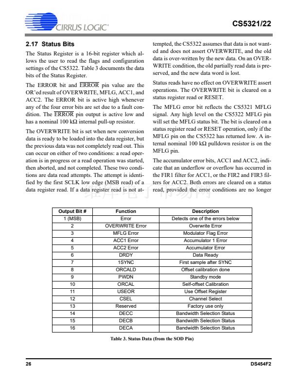
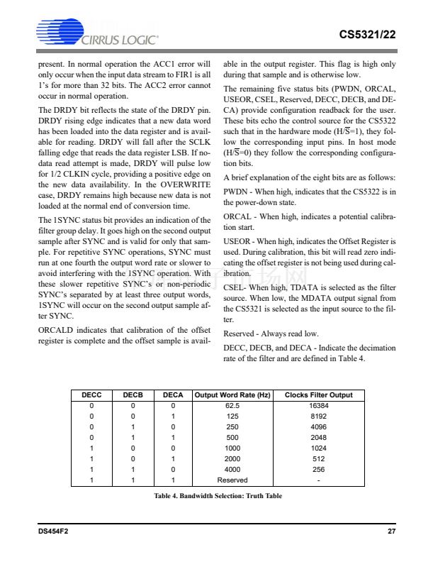
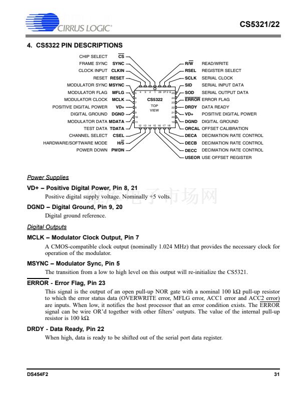
CS5321/22
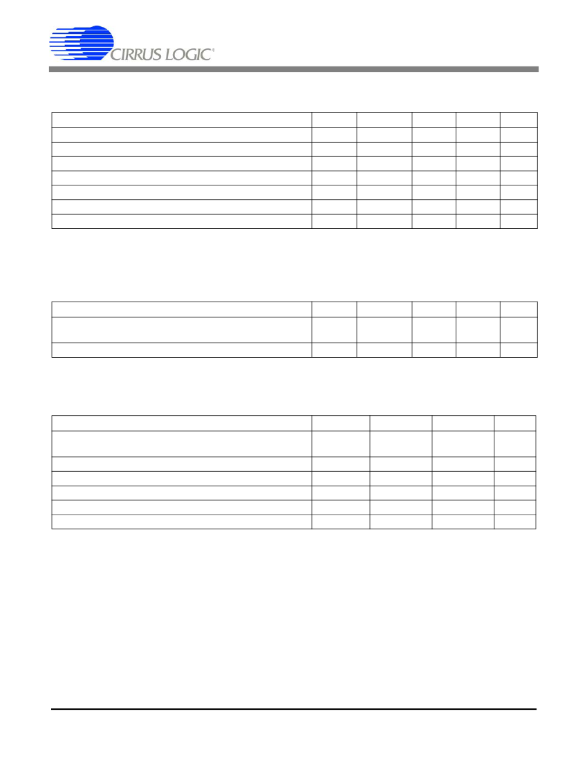
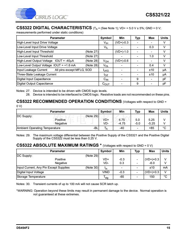
CS5321 DIGITAL CHARACTERISTICS
(T
A
= (See Note 1); V
dd1
= V
dd2
0 V; measurements performed under static conditions)
Parameter
High-Level Input Drive Voltage
Low-Level Input Drive Voltage
High-Level Output Voltage IOUT = -40 碌A
Low-Level Output Voltage IOUT = +40 碌A
Input Leakage Current
Digital Input Capacitance
Digital Output Capacitance
(Note 18)
(Note 18)
(Note 19)
(Note 19)
Symbol
V
IH
V
IL
V
OH
V
OL
I
LKG
C
IN
C
OUT
Min
(V
dd
)-0.6
-
(V
dd
)-0.3
-
-
-
-
Typ
-
-
-
-
-
9
9
Max
-
1.0
-
0.3
卤10
-
-
Units
V
V
V
V
碌A
pF
pF
= 5.0 V
卤
5%; GND =
Notes: 18. Device is intended to be driven with CMOS logic levels.
19. Device is intended to be interfaced to CMOS logic. Resistive loads are not recommended on these pins.
CS5321 RECOMMENDED OPERATION CONDITIONS
(Voltages with respect to GND =
0 V, See Note 20)
Parameter
DC Supply:
Ambient Operating Temperature
Symbol
Positive V
dd1,
V
dd2
Negative V
ss1
,V
ss2
-BL
T
A
Min
4.75
-4.75
-55
Typ
5.0
-5.0
-
Max
5.25
-5.25
+85
Units
V
V
掳C
Notes: 20. The maximum voltage differential between the Positive Supply of the CS5321 and the Positive Digital
Supply of the CS5322 must be less than 0.25 V.
CS5321 ABSOLUTE MAXIMUM RATINGS *
(Voltages with respect to GND = 0 V)
Parameter
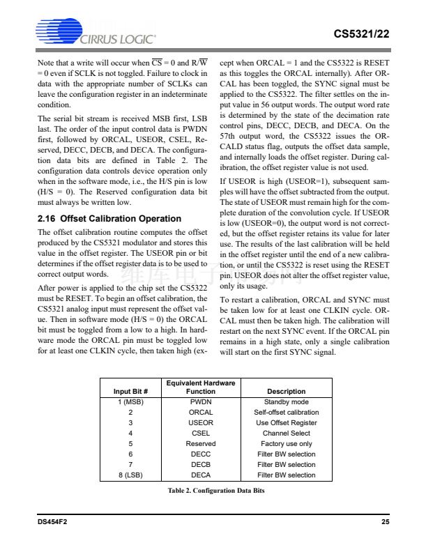
DC Supply:
Input Current, Any Pin Except Supplies
Output Current
Total Power (all supplies and outputs)
Digital Input Voltage
Storage Temperature
Positive
Negative
(Note 21)
Symbol
V
dd1,
V
dd2
V
ss1
,V
ss2
I
in
I
out
P
t
V
IND
T
stg
Min
-0.3
+0.3
-
-
-
-0.3
-65
Max
6.0
-6.0
卤10
25
1
(V
dd
)+0.3
150
Units
V
V
mA
mA
W
V
掳C
Notes: 21. Transient currents of up to 100 mA will not cause SCR latch up.
*WARNING: Operation beyond these limits may result in permanent damage to the device. Normal operation is
not guaranteed at these extremes.
DS454F2
7


 1
1
 2
2
 3
3
 4
4
 5
5
 6
6
 7
7
 8
8
 9
9
 10
10
 11
11
 12
12
 13
13
 14
14
 15
15
 16
16
 17
17
 18
18
 19
19
 20
20
 21
21
 22
22
 23
23
 24
24
 25
25
 26
26
 27
27
 28
28
 29
29
 30
30
 31
31
 32
32
 33
33
 34
34
 35
35
 36
36
