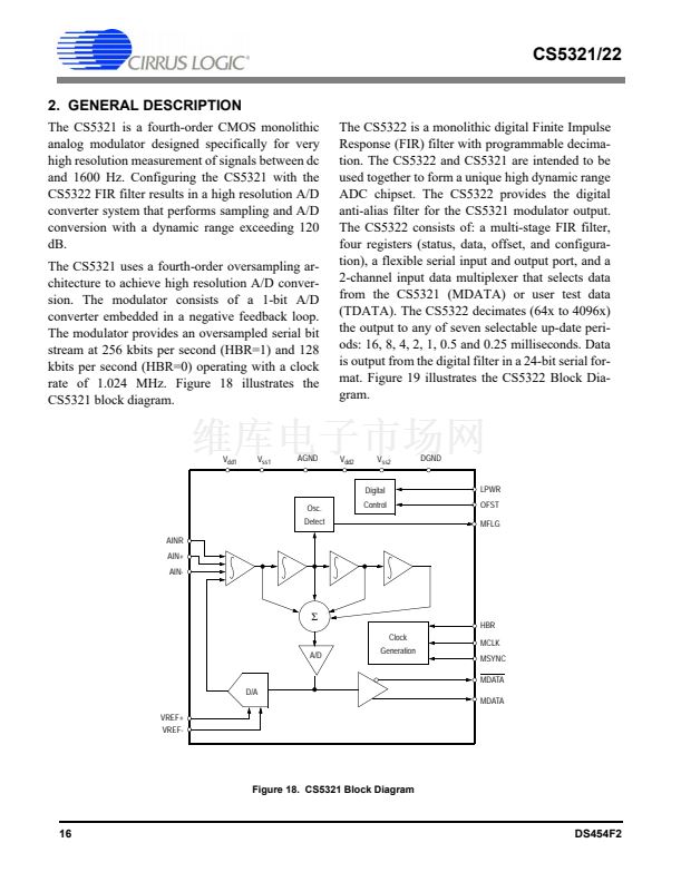
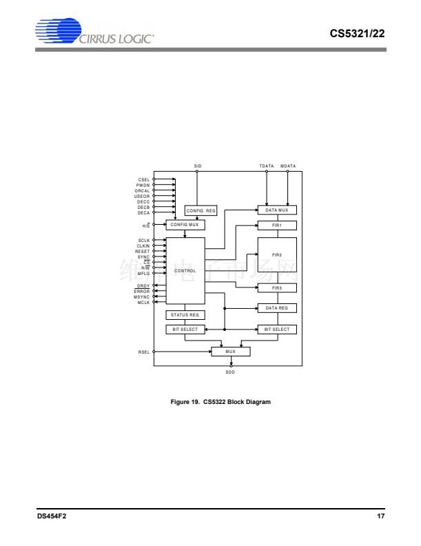
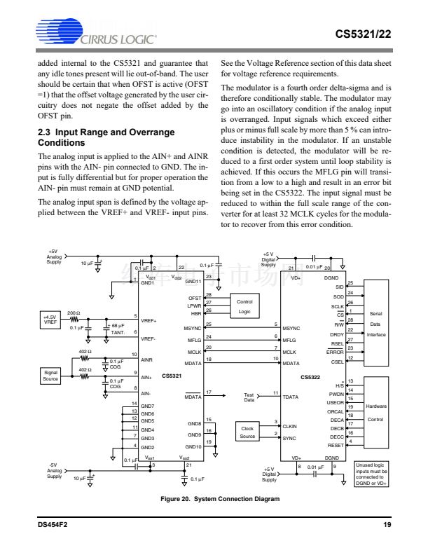
CS5321/22
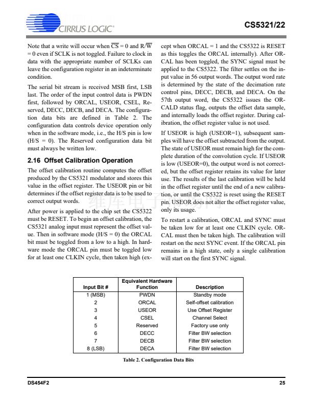
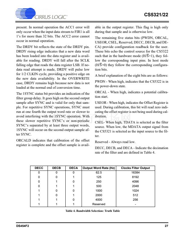
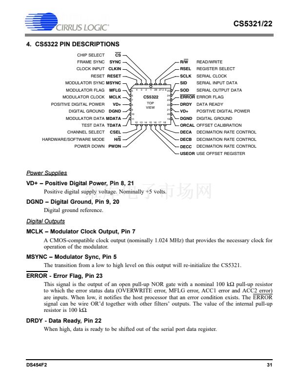
DECC - Decimation Rate Control, Pin 16
See Table 4.
H/S - Hardware/Software Mode Select, Pin 13
When high, the device pins control device operation; when low, the value entered by a prior
configuration write controls device operation.
CS - Chip Select, Pin 1
When high, all signal activity on the SID, R/W and SCLK pins is ignored. The DRDY and
ERROR signals indicate the status of the chip鈥檚 internal operation.
R/W - Read/Write, Pin 28
Used in conjunction with CS such that when both signals are low, the filter inputs data from the
SID pin on the falling edge of SCLK. If CS is low and R/W is high, the filter outputs data on
the SOD pin on the rising edge of SCLK. R/W low floats the SOD pin allowing SID and SOD
to be tied together, forming a bidirectional serial data bus.
SCLK - Serial Clock, Pin 26
Clock signal generated by host processor to either input data on the SID input pin, or output
data on the SOD output pin. For write, data must be valid on the SID pin on the falling edge of
SCLK. Data changes on the SOD pin on the rising edge of SCLK.
SID - Serial Data Input, Pin 25
Data bits are presented MSB first, LSB last. Data is latched on the falling edge of SCLK.
RSEL - Register Select, Pin 27
Selects conversion data when high, or status data when low.
USEOR - Use Offset Register, Pin 15
Use offset register value to correct output words when high. Output words will not be offset
corrected when low.
ORCAL - Offset Register Calibrate, Pin 19
Initiates an offset calibration cycle when SYNC goes high after ORCAL has been toggled from
low to high. The offset value is output on the 57th word following SYNC. Subsequent words
will have their offset correction controlled by USEOR.
DS454F2
33


 1
1
 2
2
 3
3
 4
4
 5
5
 6
6
 7
7
 8
8
 9
9
 10
10
 11
11
 12
12
 13
13
 14
14
 15
15
 16
16
 17
17
 18
18
 19
19
 20
20
 21
21
 22
22
 23
23
 24
24
 25
25
 26
26
 27
27
 28
28
 29
29
 30
30
 31
31
 32
32
 33
33
 34
34
 35
35
 36
36
