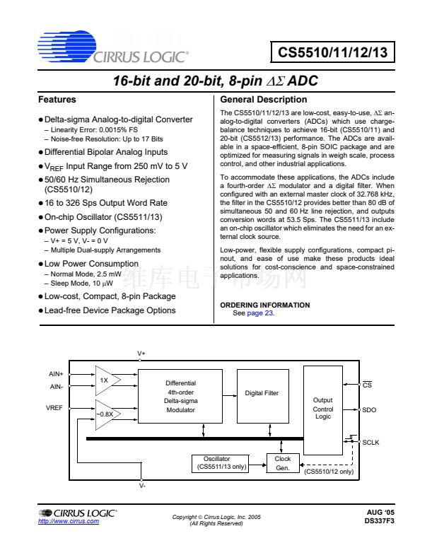
mance. The ADCs are available in a space-effi-
and other industrial applications.
鈭單?/div>
modulator and a digital fil-
ter. When configured with an external master clock
of 32.768 kHz, the filter in the CS5510/12 provides
better than 80 dB of simultaneous 50 and 60 Hz
line rejection, and outputs conversion words at
53.5 Sps. The CS5511/13 include an on-chip oscil-
lator which eliminates the need for an external
clock source.
The CS5510/11/12/13 ADCs are designed to oper-
ate from a single +5 V supply or a variety dual-sup-
ply configurations and are optimized to digitize
bipolar signals in industrial applications.
To achieve low cost, the CS5510/11/12/13 family
of converters have no on-chip calibration features.
The CS5510/11/12/13 offer very low offset drift,
low gain drift, and excellent linearity.
ferential voltage reference (VREF - V-). This trans-
lates to typically 卤4.0 V fully differential when the
reference voltage between VREF and V- is 5 V,
and typically 卤2.0 V fully differential at 2.5 V.
Note:
When a smaller reference voltage is used,
the resulting code widths are smaller. Since
the output codes exhibit more changing
codes for a fixed amount of noise, the
converter appears noisier.
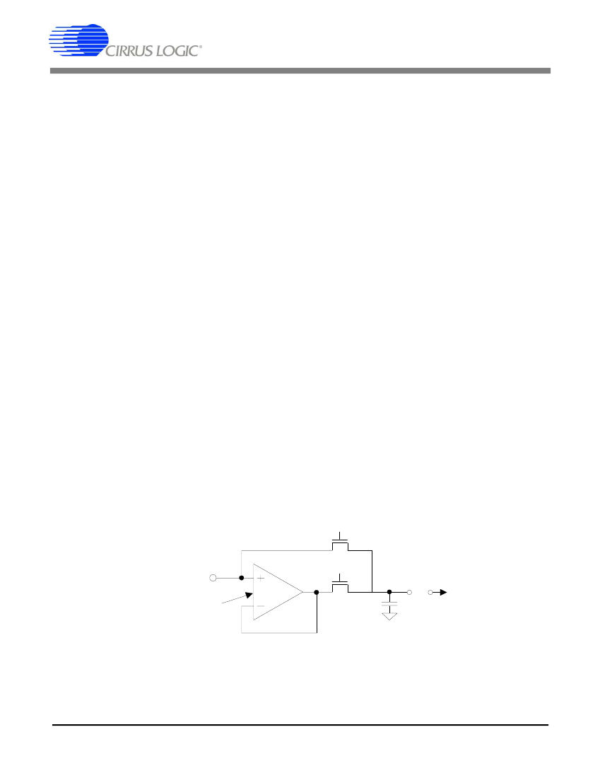
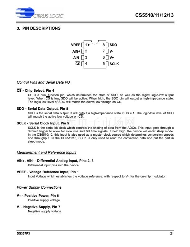
2.1.1
Analog Input Model
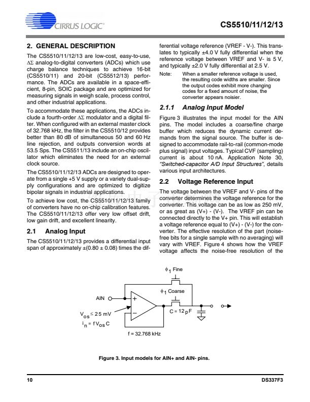
Figure 3 illustrates the input model for the AIN
pins. The model includes a coarse/fine charge
buffer which reduces the dynamic current de-
mands from the signal source. The buffer is de-
signed to accommodate rail-to-rail (common-mode
plus signal) input voltages. Typical CVF (sampling)
current is about 10 nA. Application Note 30,
鈥淪witched-capacitor A/D Input Structures鈥?
details
various input architectures.
2.2
Voltage Reference Input
2.1
Analog Input
The CS5510/11/12/13 provides a differential input
span of approximately 卤(0.80 卤 0.08) times the dif-
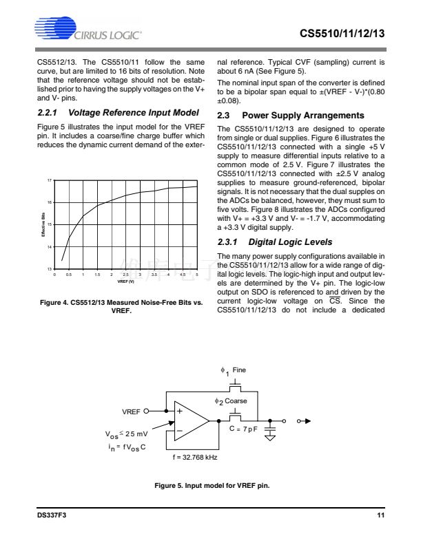
The voltage between the VREF and V- pins of the
converter determines the voltage reference for the
converter. This voltage can be as low as 250 mV,
or as great as (V+) - (V-). The VREF pin can be
connected directly to the V+ pin. This will establish
a voltage reference equal to (V+) - (V-) for the con-
verter. The effective resolution of the part (noise-
free bits for a single sample with no averaging) will
vary with VREF. Figure 4 shows how the VREF
voltage affects the noise-free resolution of the
蠁
1 Fine
蠁
1 Coarse
AIN
Vo s
鈮?/div>
2 5 mV
i n
=
f Vos C
f = 32.768 kHz
C
=
12 p F
Figure 3. Input models for AIN+ and AIN- pins.
10
DS337F3


 1
1
 2
2
 3
3
 4
4
 5
5
 6
6
 7
7
 8
8
 9
9
 10
10
 11
11
 12
12
 13
13
 14
14
 15
15
 16
16
 17
17
 18
18
 19
19
 20
20
 21
21
 22
22
 23
23
 24
24
