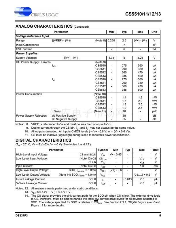
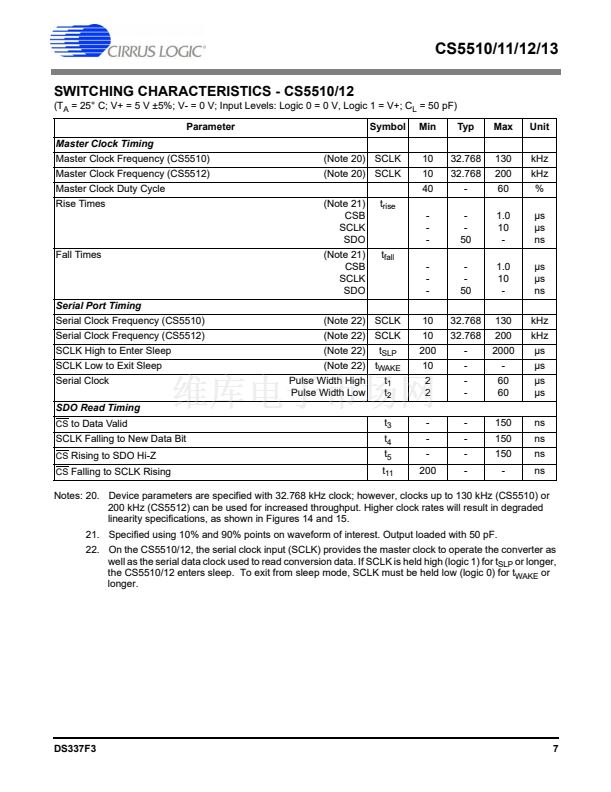
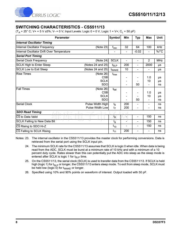
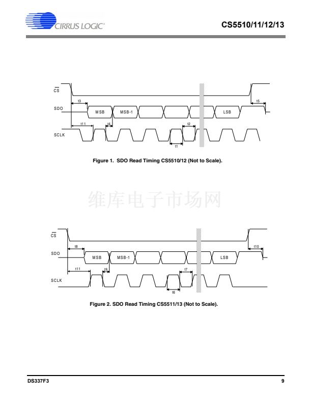
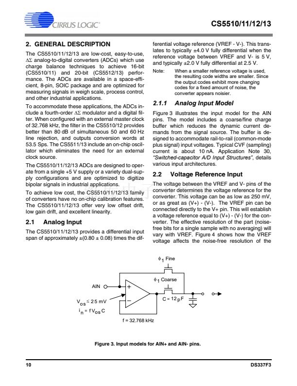
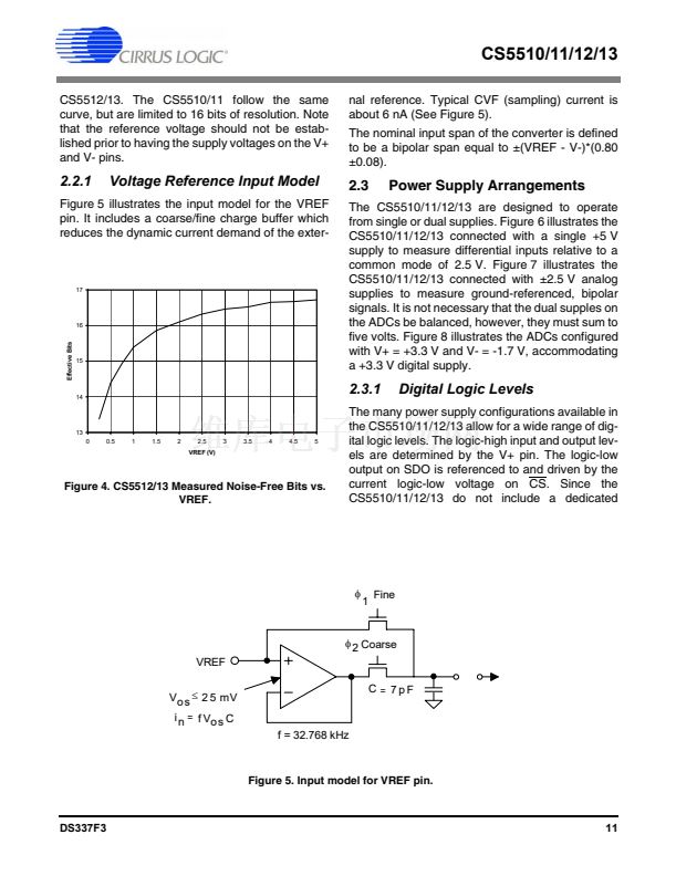
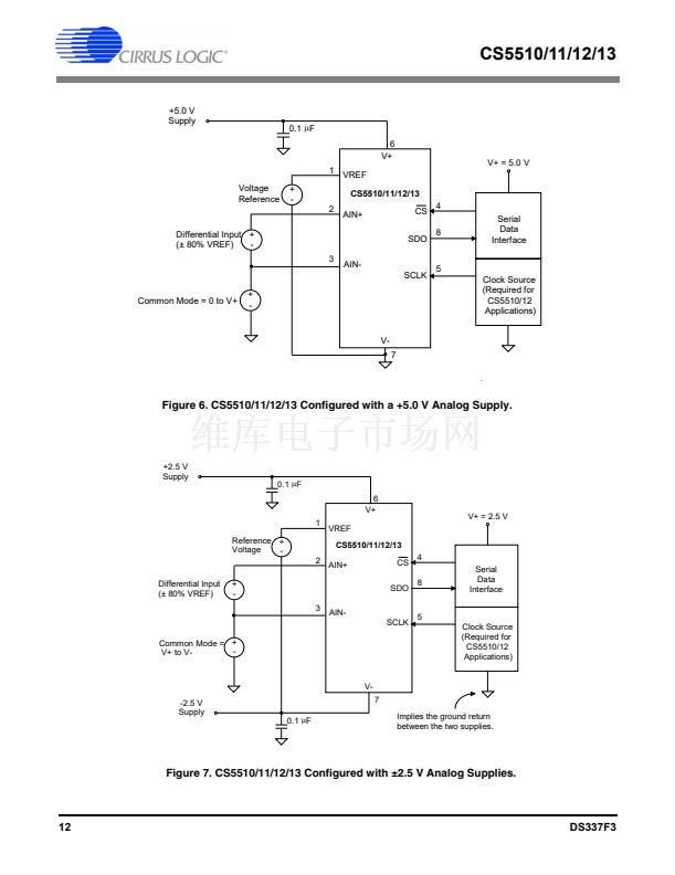
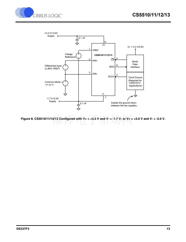
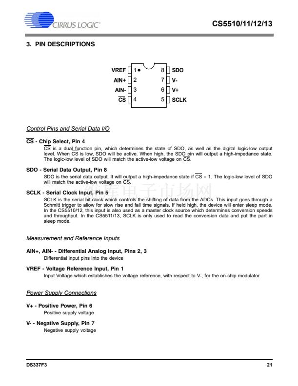
CS5510/11/12/13
priate time during the third conversion cycle to en-
sure the maximum possible throughput.
will be equivalent to: 0x7FFF*Vcal/(0.80*Vref) for
the CS5510/11, and 0x7FFFF*Vcal/(0.80*Vref) for
the CS5512/13. The gain error (GE) is equal to: (Cr
- ZP)/Ci. To correct for both offset and gain error in
subsequent conversions, subtract the offset error,
and then divide by the gain error.
2.6
Digital Off-chip System
Calibration
The CS5510/11/12/13 exhibit excellent linearity
with low offset and gain drift, without the need for
calibration. If precision voltage measurements are
required by the system, however, software-based
offset and gain calibration can be performed by the
system.
To perform a software offset calibration, the 鈥渮ero-
point鈥?of the system should be established by ap-
plying an input to the system equal to zero. Then,
the user can obtain a conversion and store it in
memory as the system鈥檚 zero point (ZP). This num-
ber can then be used as the zero point for any sub-
sequent conversion words. In the 20-bit devices
(CS5512 and CS5513), multiple conversions can
be averaged to arrive at a more accurate offset val-
ue. In the 16-bit devices (CS5510 and CS5511),
averaging may not be meaningful, because the
noise will be below the size of one LSB when using
nominal voltages for VREF (2.5 V).
A software gain calibration can be performed by
bringing the system to a known calibration Voltage
value (Vcal) and acquiring a conversion (note that
Vcal should be low enough to compensate for the
possible gain error of the ADC). Multiple conver-
sions can be averaged at this point to improve the
accuracy of the calibration. The code obtained
from this conversion is the real value (Cr) of the
calibration Voltage input, and will differ from the
ideal value. The ideal value for this conversion (Ci)
2.7
Power Consumption, Sleep and
Reset
The CS5510/11/12/13 accommodates two power
modes:
normal
and
sleep.
The normal mode is the
default mode and is entered after power is estab-
lished to the ADC. In normal mode, the ADCs typ-
ically consumes 2.5 mW. Sleep is entered when
the user leaves SCLK high for at least 200
碌s.
The
ADCs are guaranteed to be in sleep after SCLK is
high (logic 1) for 2 ms. The sleep mode reduces
the consumed power to less than 10
碌W
when CS
is high (logic 1). If CS is low (logic 0) at this time,
the SDO drive logic will still be active, and the con-
sumed sleep power will be greater. To exit sleep
and return to normal mode, the user must return
SCLK low for at least 10
碌s.
After a sleep is exited,
the ADCs reset all their internal logic, including
their digital filters, and begin performing conver-
sions. Since the filters are reset, the first three con-
version after returning to normal mode will not be
fully settled.
2.8
PCB Layout
The CS5510/11/12/13 should be placed entirely
over the analog ground. Place the analog-digital
plane split immediately adjacent to the digital pins
of the chip.
20
DS337F3


 1
1
 2
2
 3
3
 4
4
 5
5
 6
6
 7
7
 8
8
 9
9
 10
10
 11
11
 12
12
 13
13
 14
14
 15
15
 16
16
 17
17
 18
18
 19
19
 20
20
 21
21
 22
22
 23
23
 24
24
