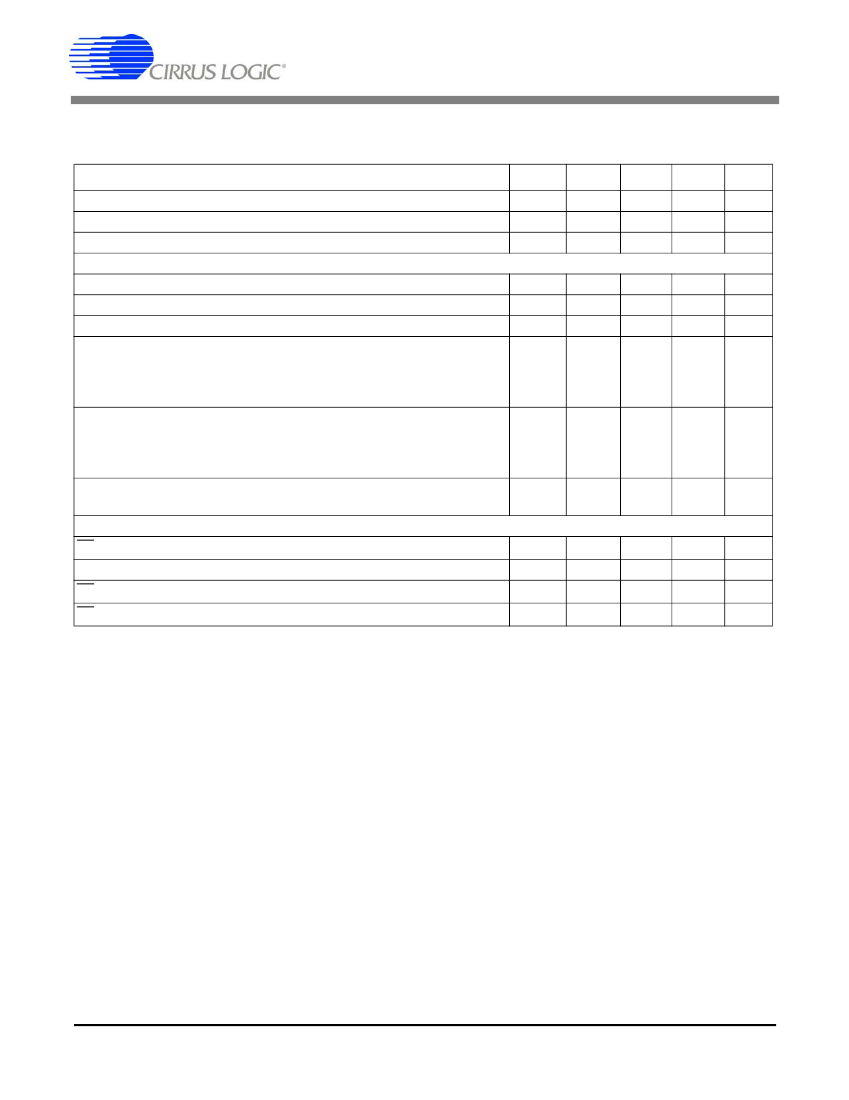
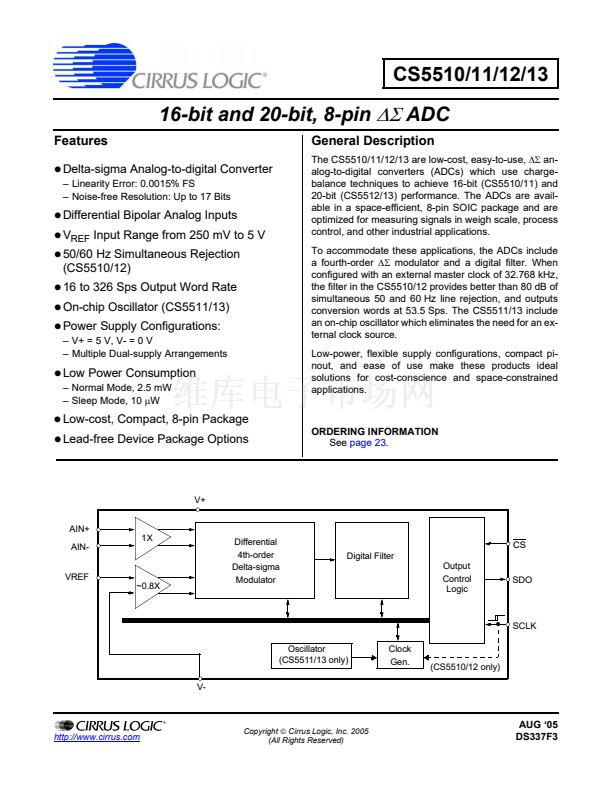
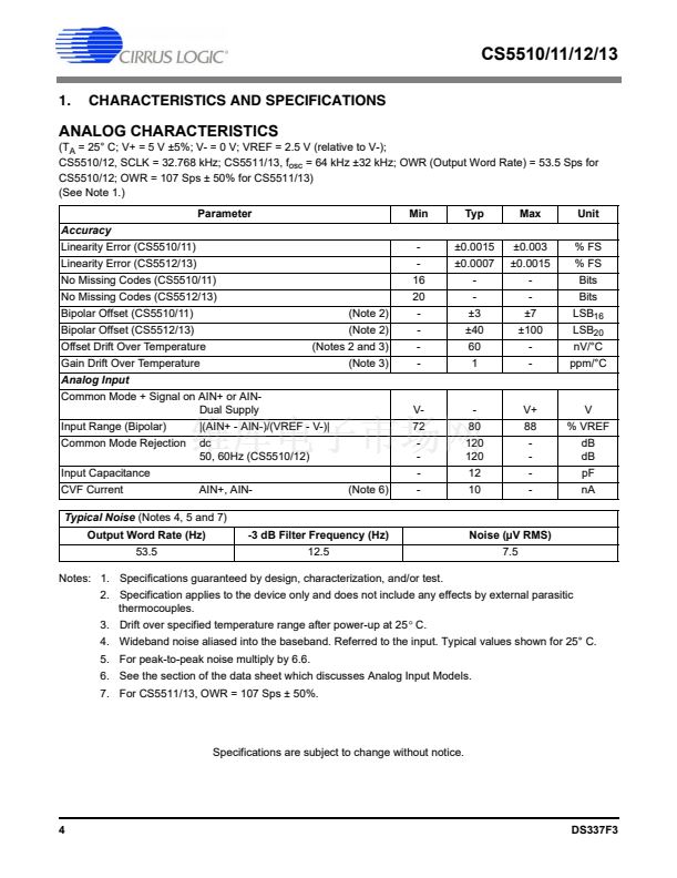
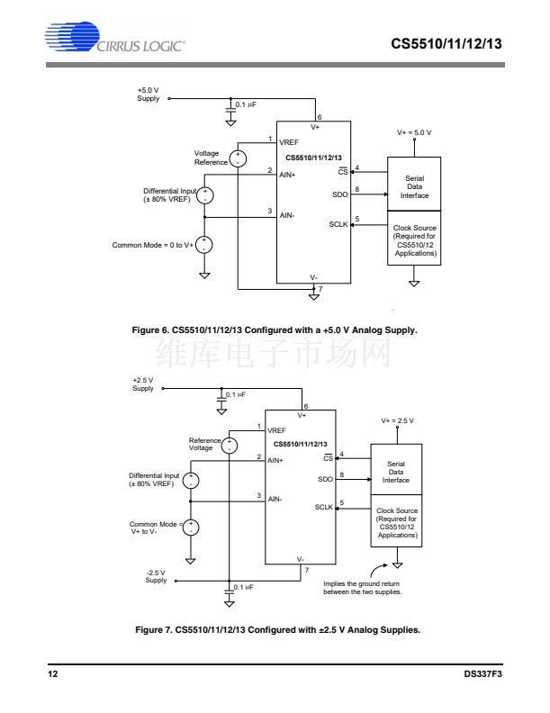
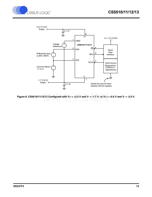
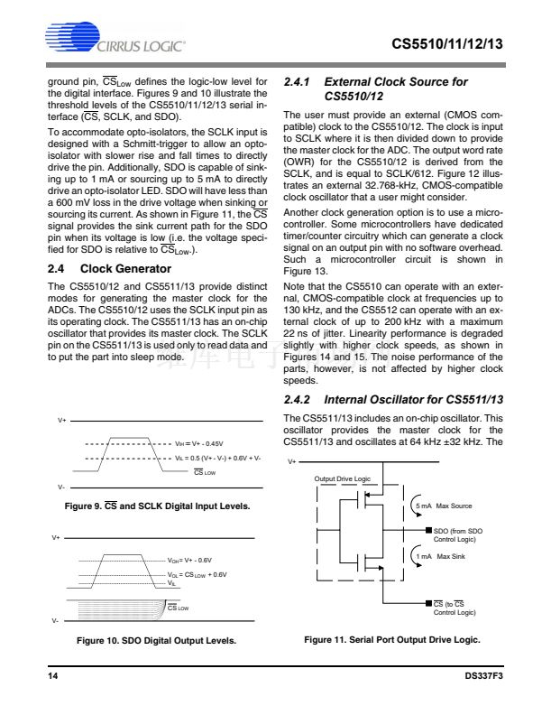
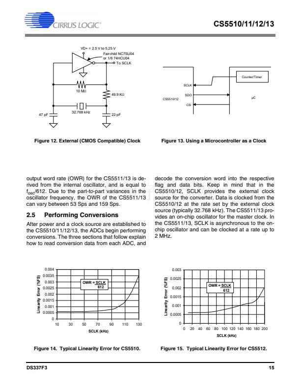
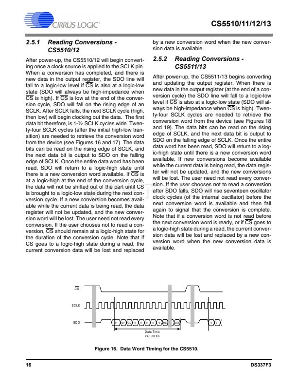
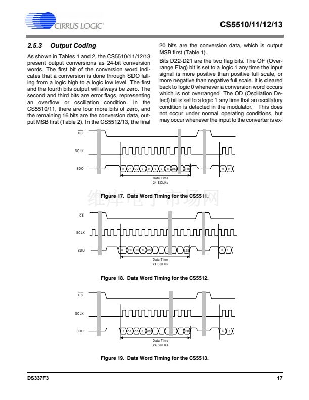
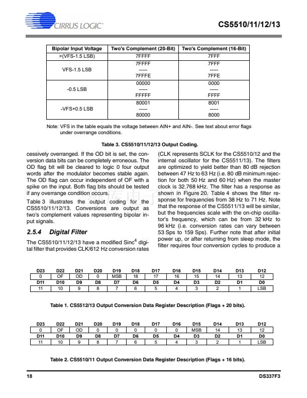
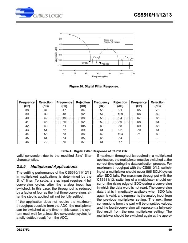
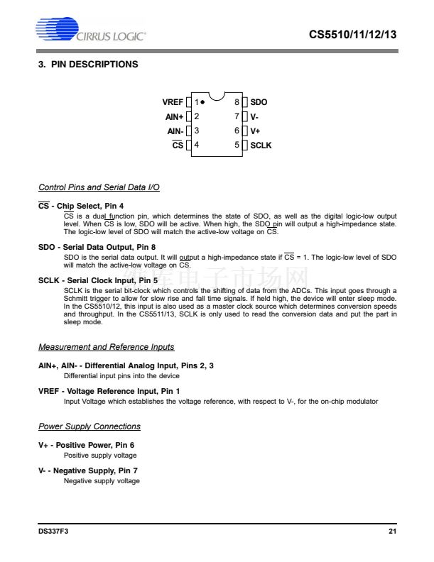
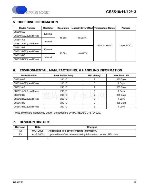
CS5510/11/12/13
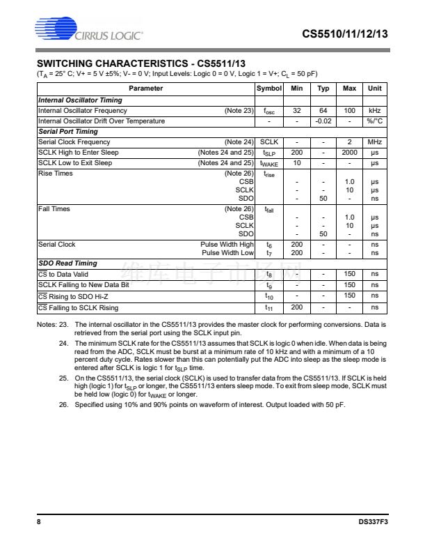
SWITCHING CHARACTERISTICS - CS5511/13
(T
A
= 25掳 C; V+ = 5 V 卤5%; V- = 0 V; Input Levels: Logic 0 = 0 V, Logic 1 = V+; C
L
= 50 pF)
Parameter
Internal Oscillator Timing
Internal Oscillator Frequency
Internal Oscillator Drift Over Temperature
Serial Port Timing
Serial Clock Frequency
SCLK High to Enter Sleep
SCLK Low to Exit Sleep
Rise Times
(Note 24) SCLK
(Notes 24 and 25)
t
SLP
(Notes 24 and 25) t
WAKE
(Note 26) t
rise
CSB
SCLK
SDO
(Note 26)
CSB
SCLK
SDO
Pulse Width High
Pulse Width Low
t
fall
-
-
-
t
6
t
7
t
8
t
9
t
10
t
11
200
200
-
-
-
200
-
-
50
-
-
-
-
-
-
1.0
10
-
-
-
150
150
150
-
碌s
碌s
ns
ns
ns
ns
ns
ns
ns
-
200
10
-
-
-
-
-
-
-
-
50
2
2000
-
1.0
10
-
MHz
碌s
碌s
碌s
碌s
ns
(Note 23)
f
osc
-
32
-
64
-0.02
100
-
kHz
%/掳C
Symbol
Min
Typ
Max
Unit
Fall Times
Serial Clock
SDO Read Timing
CS
to Data Valid
SCLK Falling to New Data Bit
CS
Rising to SDO Hi-Z
CS
Falling to SCLK Rising
Notes: 23. The internal oscillator in the CS5511/13 provides the master clock for performing conversions. Data is
retrieved from the serial port using the SCLK input pin.
24. The minimum SCLK rate for the CS5511/13 assumes that SCLK is logic 0 when idle. When data is being
read from the ADC, SCLK must be burst at a minimum rate of 10 kHz and with a minimum of a 10
percent duty cycle. Rates slower than this can potentially put the ADC into sleep as the sleep mode is
entered after SCLK is logic 1 for t
SLP
time.
25. On the CS5511/13, the serial clock (SCLK) is used to transfer data from the CS5511/13. If SCLK is held
high (logic 1) for t
SLP
or longer, the CS5511/13 enters sleep mode. To exit from sleep mode, SCLK must
be held low (logic 0) for t
WAKE
or longer.
26. Specified using 10% and 90% points on waveform of interest. Output loaded with 50 pF.
8
DS337F3


 1
1
 2
2
 3
3
 4
4
 5
5
 6
6
 7
7
 8
8
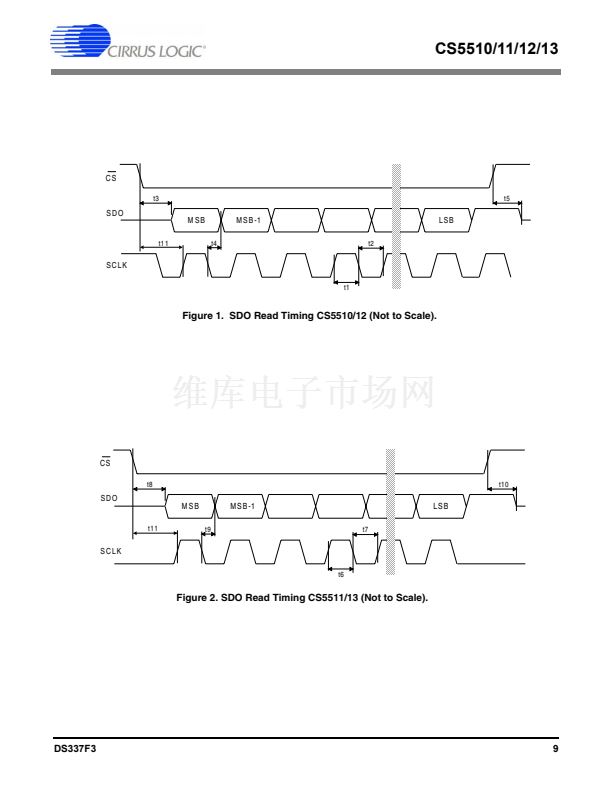 9
9
 10
10
 11
11
 12
12
 13
13
 14
14
 15
15
 16
16
 17
17
 18
18
 19
19
 20
20
 21
21
 22
22
 23
23
 24
24
