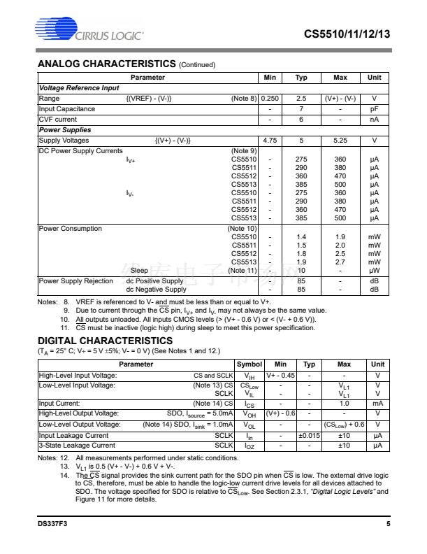
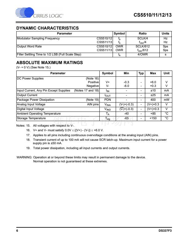
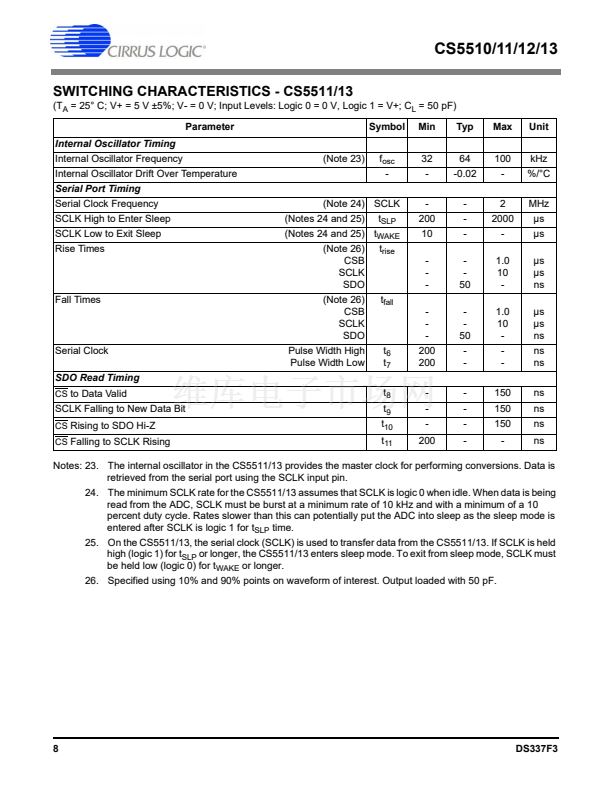
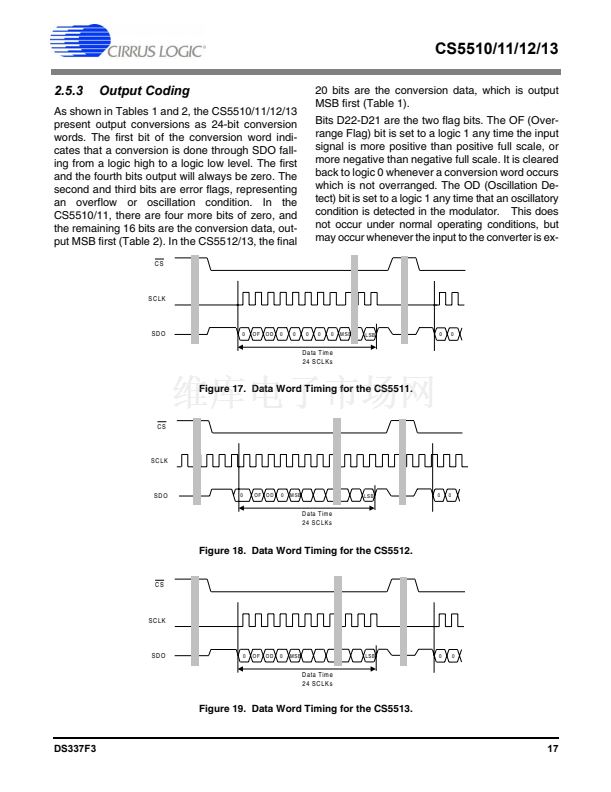
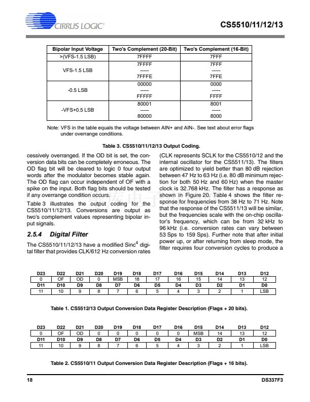
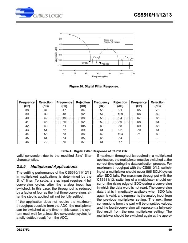
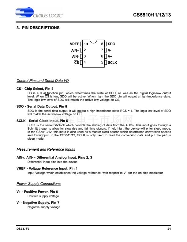
CS5510/11/12/13
ground pin, CS
Low
defines the logic-low level for
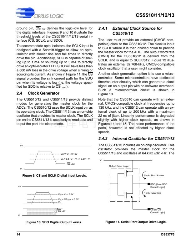
the digital interface. Figures 9 and 10 illustrate the
threshold levels of the CS5510/11/12/13 serial in-
terface (CS, SCLK, and SDO).
To accommodate opto-isolators, the SCLK input is
designed with a Schmitt-trigger to allow an opto-
isolator with slower rise and fall times to directly
drive the pin. Additionally, SDO is capable of sink-
ing up to 1 mA or sourcing up to 5 mA to directly
drive an opto-isolator LED. SDO will have less than
a 600 mV loss in the drive voltage when sinking or
sourcing its current. As shown in Figure 11, the CS
signal provides the sink current path for the SDO
pin when its voltage is low (i.e. the voltage speci-
fied for SDO is relative to CS
Low
.).
2.4.1
External Clock Source for
CS5510/12
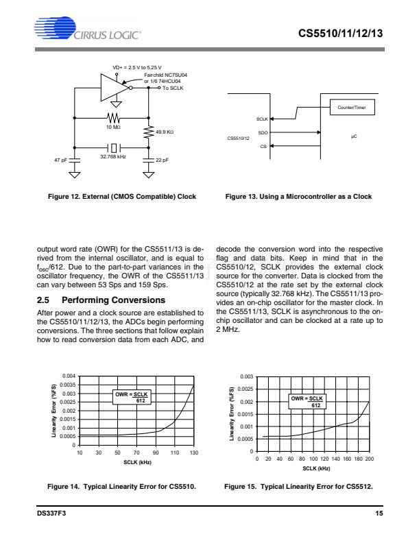
The user must provide an external (CMOS com-
patible) clock to the CS5510/12. The clock is input
to SCLK where it is then divided down to provide
the master clock for the ADC. The output word rate
(OWR) for the CS5510/12 is derived from the
SCLK, and is equal to SCLK/612. Figure 12 illus-
trates an external 32.768-kHz, CMOS-compatible
clock oscillator that a user might consider.
Another clock generation option is to use a micro-
controller. Some microcontrollers have dedicated
timer/counter circuitry which can generate a clock
signal on an output pin with no software overhead.
Such a microcontroller circuit is shown in
Figure 13.
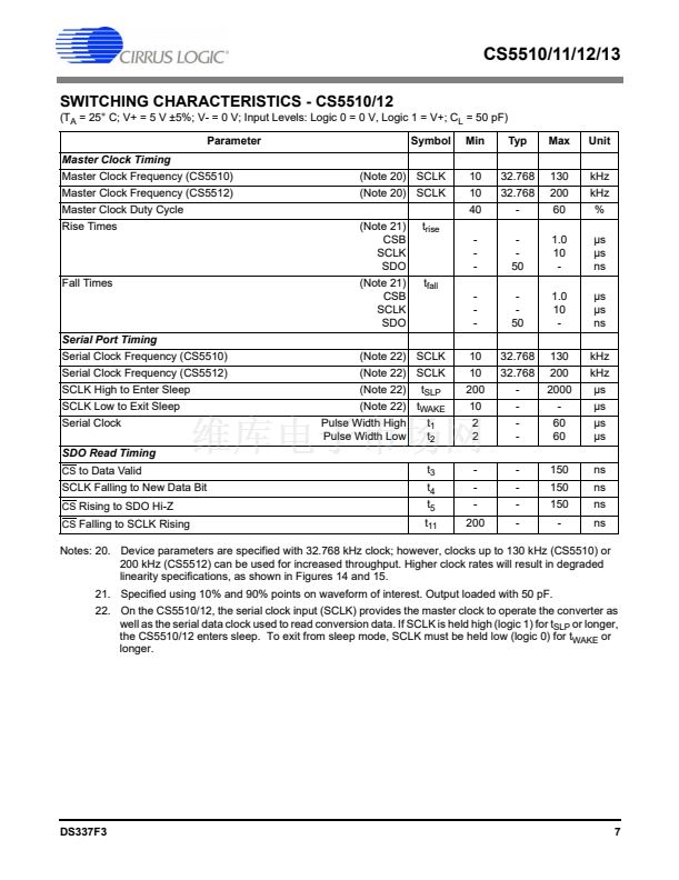
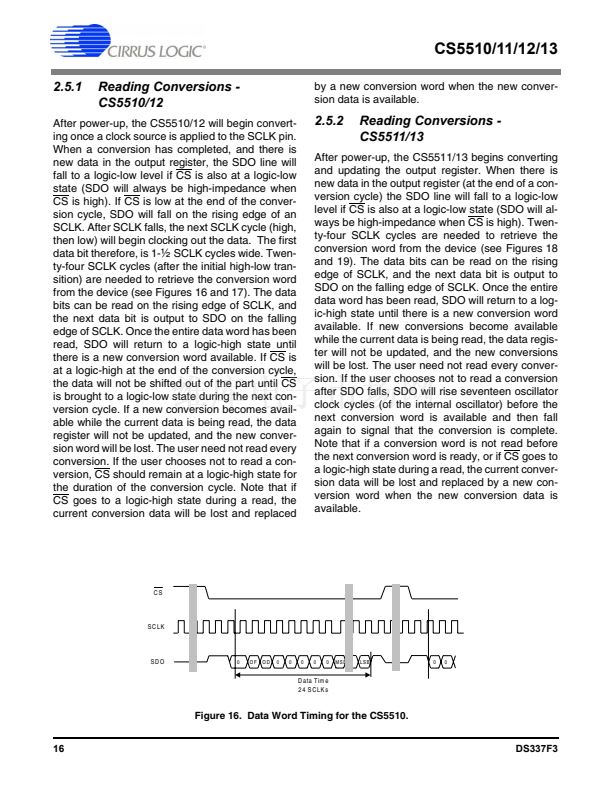
Note that the CS5510 can operate with an exter-
nal, CMOS-compatible clock at frequencies up to
130 kHz, and the CS5512 can operate with an ex-
ternal clock of up to 200 kHz with a maximum
22 ns of jitter. Linearity performance is degraded
slightly with higher clock speeds, as shown in
Figures 14 and 15. The noise performance of the
parts, however, is not affected by higher clock
speeds.
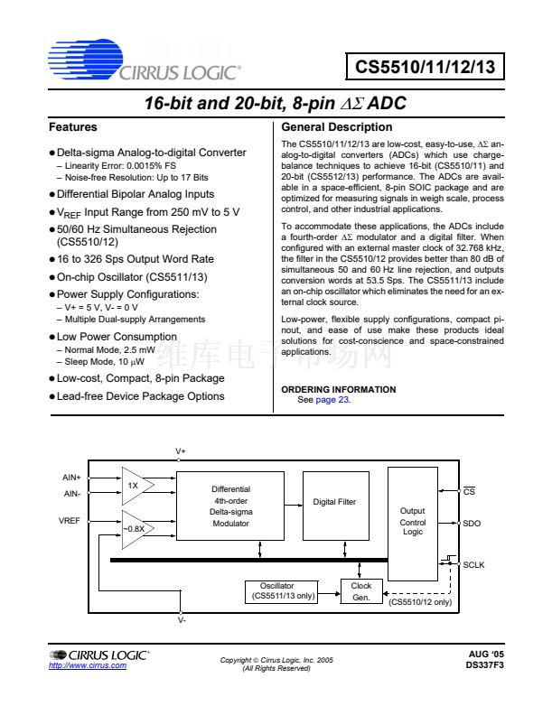
2.4
Clock Generator
The CS5510/12 and CS5511/13 provide distinct
modes for generating the master clock for the
ADCs. The CS5510/12 uses the SCLK input pin as
its operating clock. The CS5511/13 has an on-chip
oscillator that provides its master clock. The SCLK
pin on the CS5511/13 is used only to read data and
to put the part into sleep mode.
2.4.2
V+
Internal Oscillator for CS5511/13
=
V
IH
= V+
- 0.45V
V
IL
= 0.5 ( V+ - V-) + 0.6V + V-
CS
LOW
V-
The CS5511/13 includes an on-chip oscillator. This
oscillator provides the master clock for the
CS5511/13 and oscillates at 64 kHz 卤32 kHz. The
V+
Output Drive Logic
Figure 9. CS and SCLK Digital Input Levels.
5 mA Max Source
V+
SDO (from SDO
Control Logic)
V
OH
= V+ - 0.6V
1 mA Max Sink
V
OL
= CS
LOW
+ 0.6V
V
IL
CS
LOW
V-
CS (to CS
Control Logic)
Figure 10. SDO Digital Output Levels.
Figure 11. Serial Port Output Drive Logic.
14
DS337F3


 1
1
 2
2
 3
3
 4
4
 5
5
 6
6
 7
7
 8
8
 9
9
 10
10
 11
11
 12
12
 13
13
 14
14
 15
15
 16
16
 17
17
 18
18
 19
19
 20
20
 21
21
 22
22
 23
23
 24
24
