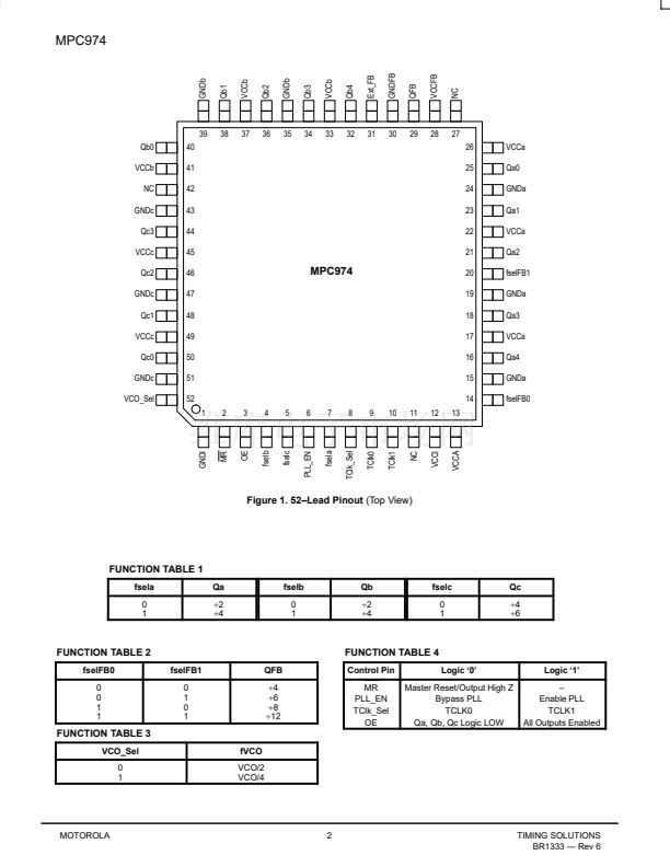
MPC974
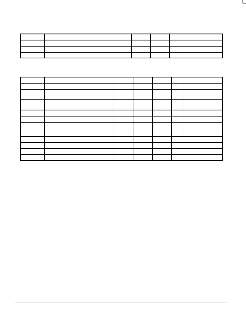
PLL INPUT REFERENCE CHARACTERISTICS
(TA = 0 to 70掳C)
Symbol
tr, tf
fref
frefDC
Characteristic
TCLK Input Rise/Falls
Reference Input Frequency
Reference Input Duty Cycle
Note 3.
25
Min
Max
3.0
Note 3.
75
Unit
ns
MHz
%
Condition
3. Input reference frequency is limited by the divider selection and the VCO lock range.
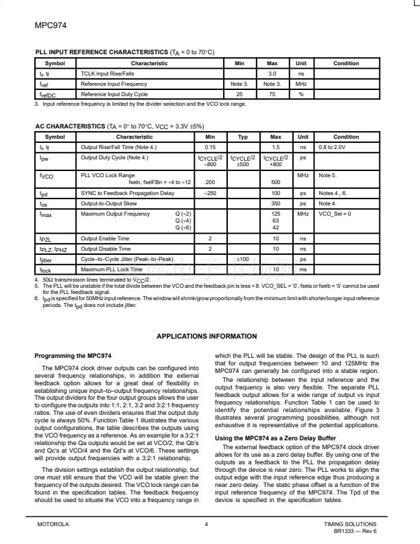
AC CHARACTERISTICS
(TA = 0掳 to 70掳C, VCC = 3.3V
卤5%)
Symbol
tr, tf
tpw
fVCO
tpd
tos
fmax
Characteristic
Output Rise/Fall Time (Note 4.)
Output Duty Cycle (Note 4.)
PLL VCO Lock Range
fseln, fselFBn =
梅4
to
梅12
SYNC to Feedback Propagation Delay
Output-to-Output Skew
Maximum Output Frequency
Q (梅2)
Q (梅4)
Q (梅6)
2
2
卤100
10
Min
0.15
tCYCLE/2
鈥?00
200
鈥?50
tCYCLE/2
卤500
Typ
Max
1.5
tCYCLE/2
+800
500
100
350
125
63
42
10
10
ps
ps
MHz
Notes 4., 6.
Note 4.
VCO_Sel = 0
Unit
ns
ps
MHz
Note 5.
Condition
0.8 to 2.0V
tPZL
tPLZ, tPHZ
tjitter
tlock
Output Enable Time
Output Disable Time
Cycle鈥搕o鈥揅ycle Jitter (Peak鈥搕o鈥揚eak)
Maximum PLL Lock Time
ns
ns
ps
ms
4. 50鈩?transmission lines terminated to VCC/2.
5. The PLL will be unstable if the total divide between the VCO and the feedback pin is less < 8. VCO_SEL = 鈥?鈥? fsela or fselb = 鈥?鈥?cannot be used
for the PLL feedback signal.
6. tpd is specified for 50MHz input reference. The window will shrink/grow proportionally from the minimum limit with shorter/longer input reference
periods. The tpd does not include jitter.
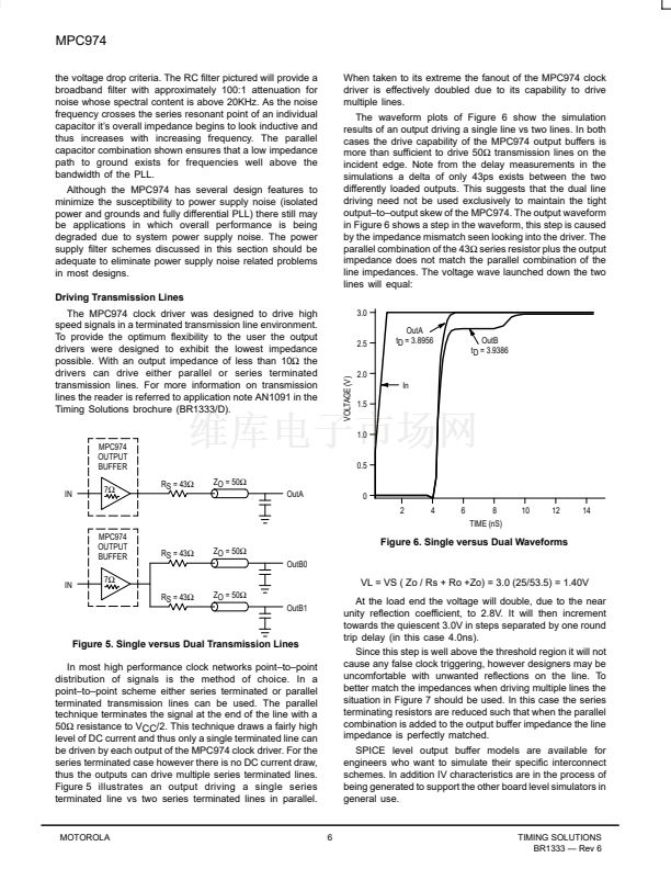
APPLICATIONS INFORMATION
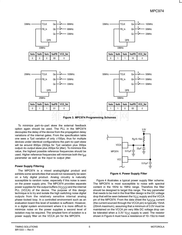
Programming the MPC974
The MPC974 clock driver outputs can be configured into
several frequency relationships, in addition the external
feedback option allows for a great deal of flexibility in
establishing unique input鈥搕o鈥搊utput frequency relationships.
The output dividers for the four output groups allows the user
to configure the outputs into 1:1, 2:1, 3:2 and 3:2:1 frequency
ratios. The use of even dividers ensures that the output duty
cycle is always 50%. Function Table 1 illustrates the various
output configurations, the table describes the outputs using
the VCO frequency as a reference. As an example for a 3:2:1
relationship the Qa outputs would be set at VCO/2, the Qb鈥檚
and Qc鈥檚 at VCO/4 and the Qd鈥檚 at VCO/6. These settings
will provide output frequencies with a 3:2:1 relationship.
The division settings establish the output relationship, but
one must still ensure that the VCO will be stable given the
frequency of the outputs desired. The VCO lock range can be
found in the specification tables. The feedback frequency
should be used to situate the VCO into a frequency range in
which the PLL will be stable. The design of the PLL is such
that for output frequencies between 10 and 125MHz the
MPC974 can generally be configured into a stable region.
The relationship between the input reference and the
output frequency is also very flexible. The separate PLL
feedback output allows for a wide range of output vs input
frequency relationships. Function Table 1 can be used to
identify the potential relationships available. Figure 3
illustrates several programming possibilities, although not
exhaustive it is representative of the potential applications.
Using the MPC974 as a Zero Delay Buffer
The external feedback option of the MPC974 clock driver
allows for its use as a zero delay buffer. By using one of the
outputs as a feedback to the PLL the propagation delay
through the device is near zero. The PLL works to align the
output edge with the input reference edge thus producing a
near zero delay. The static phase offset is a function of the
input reference frequency of the MPC974. The Tpd of the
device is specified in the specification tables.
MOTOROLA
4
TIMING SOLUTIONS
BR1333 鈥?Rev 6


 1
1
 2
2
 3
3
 4
4
 5
5
 6
6
 7
7
 8
8
 9
9
