3.0V/3.3V Adjustable Microprocessor
Supervisory Circuits
MAX793/MAX794/MAX795
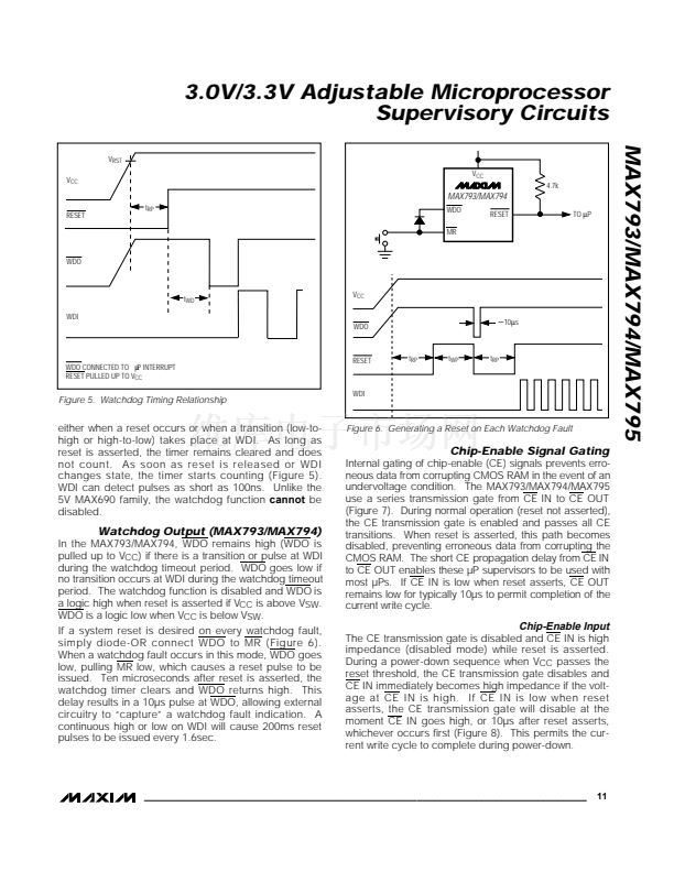
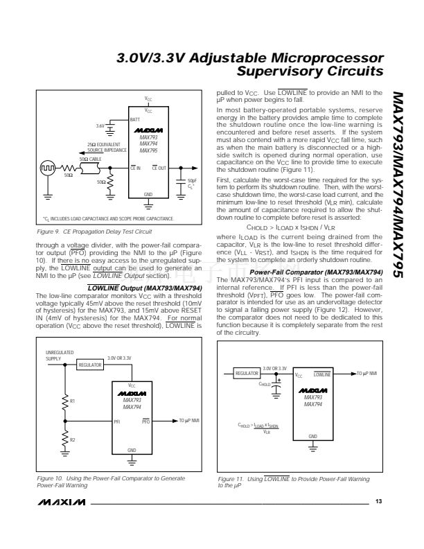
The propagation delay through the CE transmission
gate depends on V
CC
, the source impedance of the
drive connected to CE IN, and the loading on CE OUT
(see the Chip-Enable Propagation Delay vs. CE OUT
Load Capacitance graph in the
Typical Operating
Characteristics).
The CE propagation delay is produc-
tion tested from the 50% point on CE IN to the 50%
point on CE OUT using a 50鈩?driver and 50pF of load
capacitance (Figure 9). For minimum propagation
delay, minimize the capacitive load at CE OUT, and
use a low-output-impedance driver.
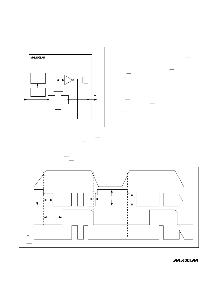
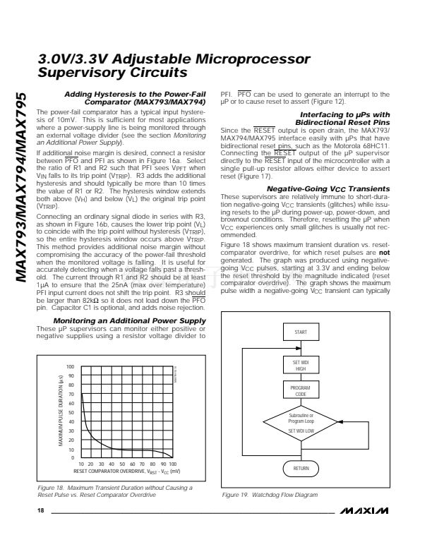
CE OUT
MAX793
MAX794
MAX795
CHIP-ENABLE
OUTPUT
CONTROL
RESET
GENERATOR
CE IN
OUT
P
P
N
Chip-Enable Output
When the CE transmission gate is enabled, the imped-
ance of CE OUT is equivalent to a 46鈩?resistor in series
with the source driving CE IN. In the disabled mode,
the transmission gate is off and an active pull-up con-
nects CE OUT to OUT (Figure 8). This pull-up turns off
when the transmission gate is enabled.
Early Power-Fail Warning
(MAX793/MAX794)
Figure 7. Chip-Enable Transmission Gate
The CE transmission gate remains disabled and CE IN
remains high impedance (regardless of CE IN activity)
for the first half of the reset timeout period (t
RP
/ 2), any
time a reset is generated. While disabled, CE IN is
high impedance. When the CE transmission gate is
enabled, the impedance of CE IN appears as a 46鈩?/div>
resistor in series with the load at CE OUT.
V
RST
V
CC
V
SW
V
RST
Critical systems often require an early warning indicat-
ing that power is failing. This warning provides time for
the 碌P to store vital data and take care of any additional
鈥渉ousekeeping鈥?functions, before the power supply
gets too far out of tolerance for the 碌P to operate reli-
ably. The MAX793/MAX794 offer two methods of
achieving this early warning. If access to the unregu-
lated supply is feasible, the power-fail comparator input
(PFI) can be connected to the unregulated supply
V
RST
V
RST
V
SW
CE OUT
V
BATT
t
RP
/
2
10碌s
V
BATT
V
CC
t
RP
RESET
(PULLED TO V
CC
)
CE IN
V
BATT
= 3.6V
RESET PULLED UP TO V
CC
Figure 8. Chip-Enable Timing
12
______________________________________________________________________________________


 1
1
 2
2
 3
3
 4
4
 5
5
 6
6
 7
7
 8
8
 9
9
 10
10
 11
11
 12
12
 13
13
 14
14
 15
15
 16
16
 17
17
 18
18
 19
19
 20
20
