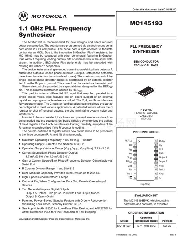
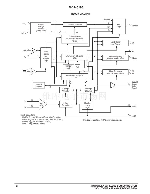
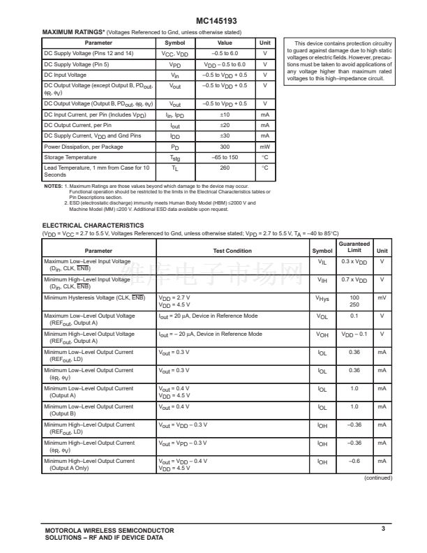
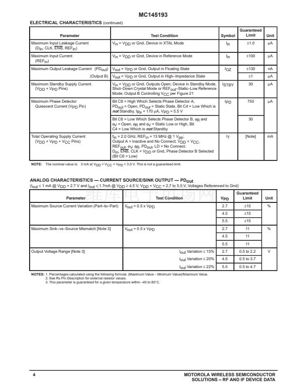
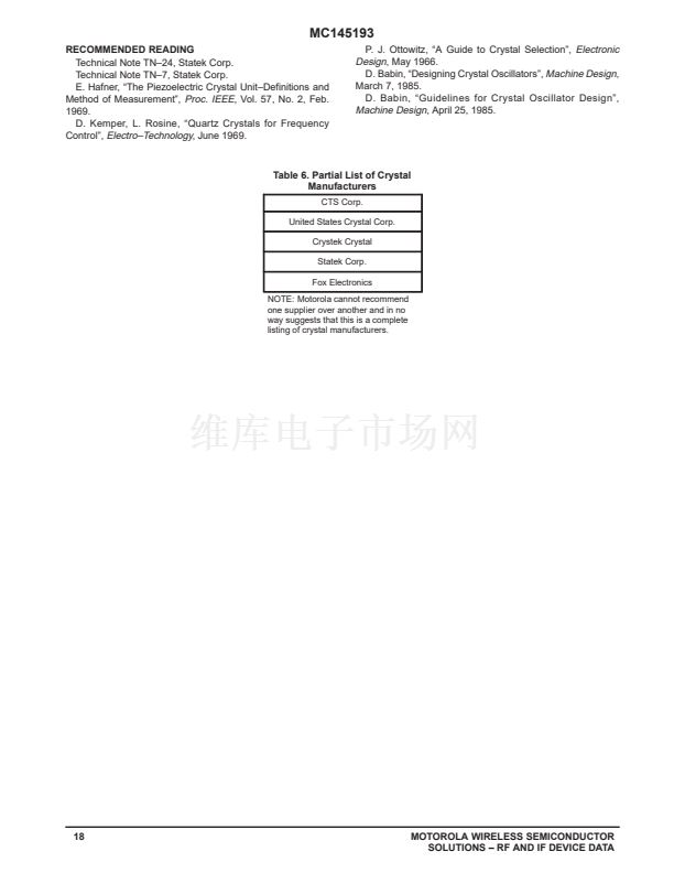
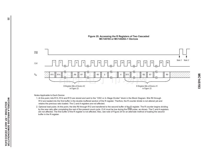
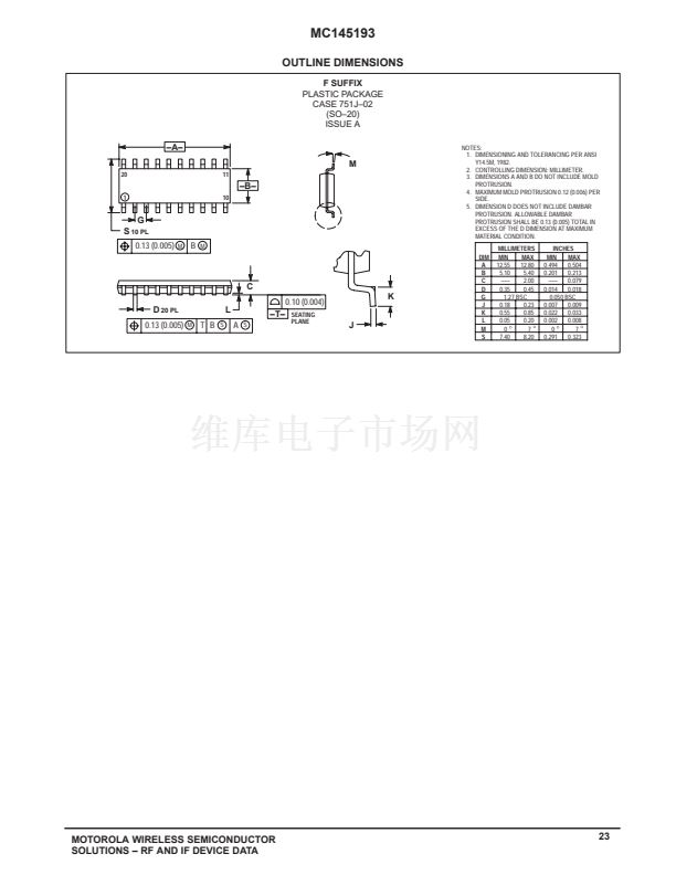
MC145193
Output A
Configurable Digital Output (Pin 16)
Output A is selectable as fR, fV, Data Out, or Port. Bits A22
and A23 in the A register control the selection; see Figure 15.
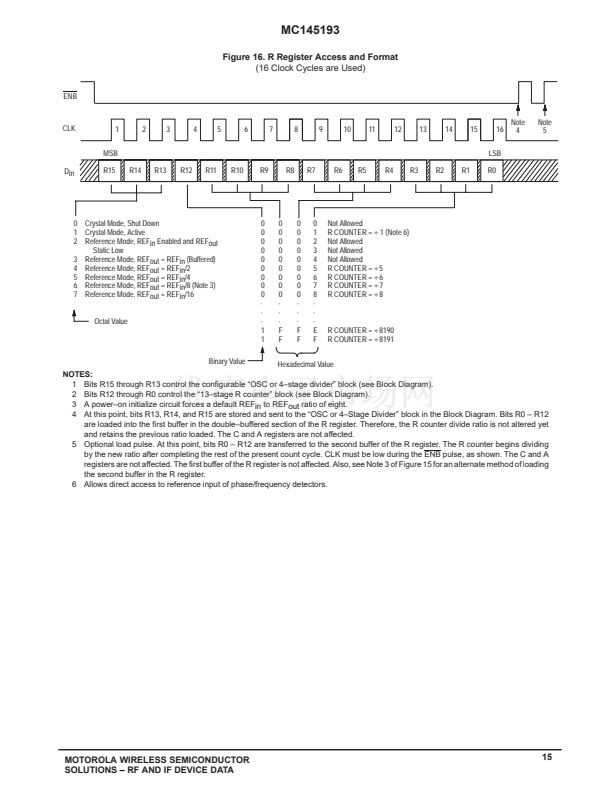
If A23 = A22 = high, Output A is configured as fR. This
signal is the buffered output of the 13鈥搒tage R counter. The
fR signal appears as normally low and pulses high. The fR
signal can be used to verify the divide ratio of the R counter.
This ratio extends from 5 to 8191 and is determined by the
binary value loaded into bits R0鈥揜12 in the R register. Also,
direct access to the phase detectors via the REFin pin is
allowed by choosing a divide value of 1 (see Figure 16). The
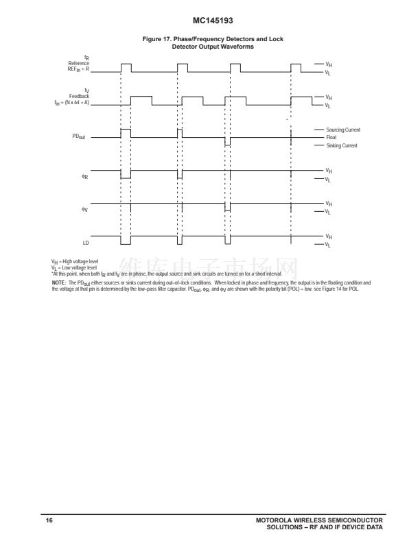
maximum frequency at which the phase detectors operate is
2 MHz. Therefore, the frequency of fR should not exceed
2 MHz.
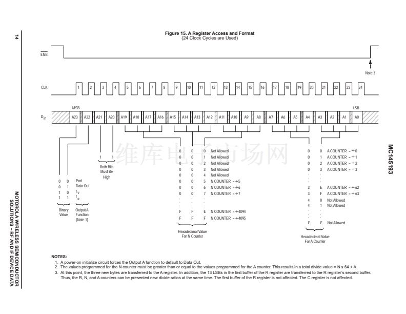
If A23 = high and A22 = low, Output A is configured as fV.
This signal is the buffered output of the 12鈥搒tage N counter.
The fV signal appears as normally low and pulses high. The
fV signal can be used to verify the operation of the prescaler,
A counter, and N counter. The divide ratio between the fin
input and the fV signal is N
脳
64 + A. N is the divide ratio of the
N counter and A is the divide ratio of the A counter. These
ratios are determined by bits loaded into the A register. See
Figure 15. The maximum frequency at which the phase
detectors operate is 2 MHz. Therefore, the frequency of fV
should not exceed 2 MHz.
If A23 = low and A22 = high, Output A is configured as
Data Out. This signal is the serial output of the 24鈥?/2鈥搒tage
shift register. The bit stream is shifted out on the high鈥搕o鈥搇ow
transition of the CLK input. Upon power up, Output A is
automatically configured as Data Out to facilitate cascading
devices.
If A23 = A22 = low, Output A is configured as Port. This
signal is a general鈥損urpose digital output which may be used
as an MCU port expander. This signal is low when the Port bit
(C1) of the C register is low, and high when the Port bit is
high.
Output B
Open鈥揇rain Digital Output (Pin 15)
This signal is a general鈥損urpose digital output which may
be used as an MCU port expander. This signal is low when
the Out B bit (C0) of the C register is low. When the Out B bit
is high, Output B assumes the high鈥搃mpedance state. Output
B may be pulled up through an external resistor or active
circuitry to any voltage less than or equal to the potential of
the VPD pin.
Note:
the maximum voltage allowed on the VPD
pin is 5.5 V.
Upon power鈥搖p, power鈥搊n reset circuitry forces Output B
to a low level.
REFERENCE PINS
REFin and REFout
Reference Input and Reference Output (Pins 20 and 1)
Configurable pins for a Crystal or an External Reference.
This pair of pins can be configured in one of two modes: the
crystal mode or the reference mode. Bits R13, R14, and R15
in the R register control the modes as shown in Figure 16.
In crystal mode, these pins form a reference oscillator
when connected to terminals of an external parallel鈥搑esonant
crystal. Frequency鈥搒etting capacitors of appropriate values,
as recommended by the crystal supplier, are connected from
each of the two pins to ground (up to a maximum of 30 pF
each, including stray capacitance). An external resistor of
1 M鈩?to 15 M鈩?is connected directly across the pins to
ensure linear operation of the amplifier. The required
connections for the components are shown in Figure 9.
To turn on the oscillator, bits R15, R14, and R13 must have
an octal value of one (001 in binary, respectively). This is the
active鈥揷rystal mode shown in Figure 16. In this mode, the
crystal oscillator runs and the R Counter divides the crystal
frequency, unless the part is in standby. If the part is placed in
standby via the C register, the oscillator runs, but the R
counter is stopped. However, if bits R15 to R13 have a value
of 0, the oscillator is stopped, which saves additional power.
This is the shut鈥揹own crystal mode (shown in Figure 16) and
can be engaged whether in standby or not.
In the reference mode, REFin (Pin 20) accepts a signal
from an external reference oscillator, such as a TCXO. A
signal swinging from at least the VIL to VIH levels listed in the
Electrical Characteristics table may be directly coupled to the
pin. If the signal is less than this level, ac coupling must be
used as shown in Figure 8. Due to an on鈥揵oard resistor
which is engaged in the reference modes, an external biasing
resistor tied between REFin and REFout is not required.
With the reference mode, the REFout pin is configured as
the output of a divider. As an example, if bits R15, R14, and
R13 have an octal value of seven, the frequency at REFout is
the REFin frequency divided by 16. In addition, Figure 16
shows how to obtain ratios of eight, four, and two. A ratio of
one鈥搕o鈥搊ne can be obtained with an octal value of three.
Upon power up, a ratio of eight is automatically initialized.
The maximum frequency capability of the REFout pin is listed
in the Loop Specifications table for an output swing of 1 Vpp
and 20 pF loads. Therefore, for higher REFin frequencies, the
one鈥搕o鈥搊ne ratio may not be used for this magnitude of
signal swing and loading requirements. Likewise, for REFin
frequencies above two times the highest rated frequency, the
ratio must be more than two.
The output has a special on鈥揵oard driver that has
slew鈥搑ate control. This feature minimizes interference in the
application.
If REFout is unused, an octal value of two should be used
for R15, R14, and R13 and the REFout pin should be floated.
A value of two allows REFin to be functional while disabling
REFout, which minimizes dynamic power consumption.
LOOP PINS
fin and fin
Frequency Inputs (Pins 11 and 10)
These pins are frequency inputs from the VCO. These
pins feed the on鈥揵oard RF amplifier which drives the 64/65
prescaler. These inputs may be fed differentially. However,
they are usually used in a single鈥揺nded configuration (shown
in Figure 7). Note that fin is driven while fin must be tied to
ground via a capacitor.
Motorola does not recommend driving fin while terminating
fin because this configuration is not tested for sensitivity. The
sensitivity is dependent on the frequency as shown in the
Loop Specifications table.
10
MOTOROLA WIRELESS SEMICONDUCTOR
SOLUTIONS 鈥?RF AND IF DEVICE DATA


 1
1
 2
2
 3
3
 4
4
 5
5
 6
6
 7
7
 8
8
 9
9
 10
10
 11
11
 12
12
 13
13
 14
14
 15
15
 16
16
 17
17
 18
18
 19
19
 20
20
 21
21
 22
22
 23
23
 24
24
